 Products Home
Ge Transimpedance Amplified Photodetectors
- Ge Detector Type
- Switchable Amplified Detectors with Output up to 10 V
- Wavelength Range from 800 - 1800 nm
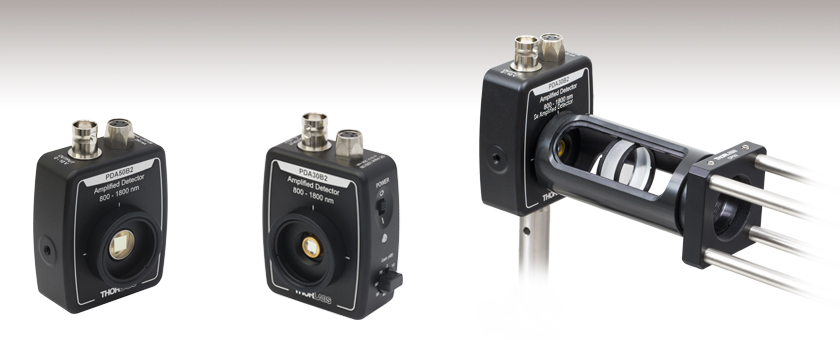
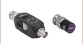
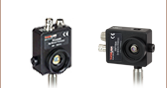
PDA50B2
Detector with Ø1" Lens
Tube Attached to a 30 mm
Cage System
Power Supply Included with Detector
PDA30B2


Please Wait

Click to Enlarge
PDA30B2 Shown with Included Power Supply

Click to Enlarge
Each detector has internal SM05 and external SM1 threads and includes an
SM1T1 Internal SM1 Adapter
and SM1RR Retaining Ring.
Features
- Detection Range: 800 - 1800 nm
- Low-Noise, Wide Band Amplifiers
- Bandwidth from DC to 510 kHz or DC to 590 kHz
- 0 to 10 V Output
- Compatible with SM1 (1.035"-40) Series and Some SM05 (0.535"-40) Series Products
- Linear Power Supply Included
Thorlabs' Germanium-based Transimpedance Amplified Photodetectors feature a switchable gain setting housed in a compact, low-profile package. These detectors are sensitive to light in the NIR spectral region from 800 nm to 1800 nm. The slim profile housing enables use in light paths with space constraints. All connections and controls are located perpendicular to the light path to provide easy accessibility when integrating the detector into a setup. Amplification is provided by a low noise transimpedance amplifier that is capable of driving 50 Ω loads. Signal output is via a BNC connector. These photodetectors can be use with Thorlabs' passive low-pass filters, which have a 50 Ω input and a high-impedance output that allows them to be directly attached to high-impedance measurement devices such as an oscilloscope. Thorlabs offers a wide variety of BNC, BNC-to-SMA, and SMC cables, as well as a variety of BNC, SMA, and SMC adapters.
Each housing features external SM1 (1.035"-40) threading, internal SM05 (0.535"-40) threading, and two universal mounting holes that accept both 8-32 and M4 threads, allowing for either vertical or horizontal post mounting. Addtionally, an SM1T1 internally threaded SM1 coupler and SM1RR retaining ring are included with each detector, allowing convenient mounting of SM1-compatible accessories, optics, and cage assembly accessories. The SM1 (1.035"-40) threading on the housing is ideally suited for mounting a Ø1" focusing lens or pinhole in front of the detector element. The internal SM05 threading is only suitable for mating to an externally threaded SM05 lens tube (components such as fiber adapters cannot be threaded onto the SM05 threading). Most SM1-threaded fiber adapters are compatible with these detectors. However, the S120-FC, S120-FC2, and S120-25 internally SM1-threaded fiber adapters are not compatible with these detectors because they collide with the photodiode. Externally SM1-threaded adapters should be mated to the included internally SM1-threaded adapter, while internally SM1-threaded adapters can be mated directly to the housing.
The active area of the detector is flush with the front of the housing, simplifying alignments within optomechanical systems. Inhomogeneities at the edges of the active area of the detector can generate unwanted capacitance and resistance effects that distort the time-domain response of the photodetector output. Thorlabs therefore recommends that the incident light on the photodetector be well-centered on the active area.
Power Supply
A ±12 V linear power supply is included with each amplified photodetector and also available separately below. The power supply features a three-way switch and can be plugged into any 50 to 60 Hz, 100 V / 120 V / 230 V power outlet. Before connecting the power supply to an outlet or to the detector, make sure that the power switches on both the power supply and detector are in the off position. Hot-plugging is not recommended.
Performance Specifications
| Item # | Detector Element |
Active Area | Wavelength | Peak Response (Typical) |
Bandwidth | NEP Rangea | Rise Timeb |
|---|---|---|---|---|---|---|---|
| PDA50B2 | Ge | 19.6 mm2 (Ø5.0 mm) |
800 - 1800 nm | 0.85 A/W @ 1550 nm |
DC - 510 kHz | 4.63 x 10⁻¹² to 1.76 x 10⁻¹⁰ W/Hz1/2 |
N/A |
| PDA30B2 | 7.1 mm2 (Ø3.0 mm) |
800 - 1800 nm | 0.85 A/W @ 1550 nm |
DC - 590 kHz | 5.93 x 10⁻¹² to 1.44 x 10⁻¹⁰ W/Hz1/2 |
N/A |
Gain Specifications
| Item # | Gain Type | Gain Step (dB) |
Gain w/ Hi-Z Load |
Gain w/ 50 Ω Load |
Bandwidtha | Noise (RMS) | NEP at Peak Wavelength |
Offset | Output Voltage w/ Hi-Z Load |
Output Voltage w/ 50 Ω Load |
|---|---|---|---|---|---|---|---|---|---|---|
| PDA50B2b | Switchable | 0 | 1.51 kV/A | 0.75 kV/A | 510 kHz | 220 µV | 1.76 x 10⁻¹⁰ W/Hz1/2 | ±15 mV (Typ.) ±20 mV (Max) |
0 - 10 V | 0 - 5 V |
| 10 | 4.75 kV/A | 2.38 kV/A | 270 kHz | 233 µV | 8.77 x 10⁻¹¹ W/Hz1/2 | |||||
| 20 | 15 kV/A | 7.5 kV/A | 85 kHz | 223 µV | 1.95 x 10⁻¹¹ W/Hz1/2 | |||||
| 30 | 47.5 kV/A | 23.8 kV/A | 22 kHz | 230 µV | 6.41 x 10⁻¹² W/Hz1/2 | |||||
| 40 | 151 kV/A | 75 kV/A | 6.3 kHz | 220 µV | 4.63 x 10⁻¹² W/Hz1/2 | |||||
| 50 | 475 kV/A | 238 kV/A | 2 kHz | 231 µV | 4.83 x 10⁻¹¹ W/Hz1/2 | |||||
| 60 | 1.5 MV/A | 750 kV/A | 630 Hz | 247 µV | 6.73 x 10⁻¹² W/Hz1/2 | |||||
| 70 | 4.75 MV/A | 2.38 MV/A | 210 Hz | 333 µV | 1.04 x 10⁻¹¹ W/Hz1/2 | |||||
| PDA30B2b | Switchable | 0 | 1.51 kV/A | 0.75 kV/A | 590 kHz | 240 µV | 1.44 x 10⁻¹⁰ W/Hz1/2 | |||
| 10 | 4.75 kV/A | 2.38 kV/A | 300 kHz | 214 μV | 6.45 x 10⁻¹¹ W/Hz1/2 | |||||
| 20 | 15 kV/A | 7.5 kV/A | 80 kHz | 212 μV | 1.24 x 10⁻¹¹ W/Hz1/2 | |||||
| 30 | 47.5 kV/A | 23.8 kV/A | 20 kHz | 211 μV | 4.25 x 10⁻¹² W/Hz1/2 | |||||
| 40 | 151 kV/A | 75 kV/A | 6 kHz | 211 μV | 3.61 x 10⁻¹² W/Hz1/2 | |||||
| 50 | 475 kV/A | 238 kV/A | 2 kHz | 212 μV | 3.56 x 10⁻¹¹ W/Hz1/2 | |||||
| 60 | 1.5 MV/A | 750 kV/A | 600 Hz | 218 μV | 4.71 x 10⁻¹² W/Hz1/2 | |||||
| 70 | 4.75 MV/A | 2.38 MV/A | 200 Hz | 243 µV | 5.93 x 10⁻¹² W/Hz1/2 |

Click to Enlarge
The power input and BNC connectors are located at the top of the housing.
Click to Enlarge
Each detector has internal SM05 and external SM1 threads and includes an
SM1T1 Internal SM1 Adapter
and SM1RR Retaining Ring.
Housing Features of the Amplified Ge Photodetectors
Thorlabs' PDA50B and PDA30B2 are compact Ge amplified photodetectors with a switchable gain. Each housing features internal SM05 (0.535"-40) threading and external SM1 (1.035"-40) threading. Each detector includes an SM1T1 internally SM1-threaded adapter and an SM1RR retaining ring. The SM1T1 can hold up to 0.1" (2.8 mm) thick optics. Each detector can be mounted using a 1/2" Post, as shown in the images below. The PDA30B2 and PDA50B2 have a housing design that features the active area flush with the front of the housing, simplifying alignments within optomechanical systems. This design also has two universal mounting holes that accept both 8-32 and M4 threads. As a convenience, the back panel is engraved with the responsivity curve of the photodiode. These switchable gain detectors feature an eight-position rotary gain switch mounted on an outside edge perpendicular to the power supply and BNC output connections. The location of the gain switch allows for easy adjustments while the detector is mounted.
Lens Tube Compatibility
These detectors can be integrated into various optomechanical systems using the internal SM05 and external SM1 threads. A lens tube can be directly attached to the SM1 threads, making the detectors compatible with lens tube systems. The SM1T1 adapter can be used to mount Ø1" (Ø25.4 mm) optical components, such as optical filters and lenses.
Cage System Compatibility
The detectors are also cage system compatible, as shown in the two images below right. A CP33(/M) cage plate can be attached directly to the SM1 threads. This attachment method does not require an adapter piece and allows the diode to be as close as possible to the cage plate, which can be important in setups where the light is divergent. Another method for integrating a detector into a cage system is using the included SM1T1 with an SM1T2 adapter. This allows more freedom in choosing the orientation of the detector. Additionally, these detectors can be used with SM1-threaded fiber adapters (sold below).
Post Mounting
Threaded holes on the housings of the detectors allow the units to be mounted in a horizontal or vertical orientation using a 1/2" Post. This gives the user the option to route the power and BNC cables from above or alongside the beam path, as shown below left.

Click to Enlarge
PDA Photodetector Mounted Horizontally

Click to Enlarge
PDA Photodetector Connected to an SM1 Lens Tube in a 30 mm Cage System

Click to Enlarge
PDA Photodetector Integrated into a 30 mm Cage System Using the External SM1 Threads

Click to Enlarge
PDA Photodetector Integrated into a 30 mm Cage System Using the SM1T1 (included) and SM1T2 Adapter
| Detectors | Housing Drawing (Click Icon for Details) |
Mounting Taps | SM Thread Compatibility | Dimensions | Output Connector |
|---|---|---|---|---|---|
| PDA50B2 | Two Universal Taps for 8-32 and M4 |
External SM1 (1.035"-40)a | 1.96" x 0.89" x 2.79" (49.8 mm x 22.5 mm x 70.9 mm) |
BNC | |
| PDA30B2 | Internal SM05 (0.535"-40) External SM1 (1.035"-40) |
BNC Female Output (Photodetector)
0 - 10 V Output
PDA Male (Power Cables)

PDA Female (Photodetector)

Photodiode Tutorial
Theory of Operation
A junction photodiode is an intrinsic device that behaves similarly to an ordinary signal diode, but it generates a photocurrent when light is absorbed in the depleted region of the junction semiconductor. A photodiode is a fast, highly linear device that exhibits high quantum efficiency and may be used in a variety of different applications.
It is necessary to be able to correctly determine the level of the output current to expect and the responsivity based upon the incident light. Depicted in Figure 100A is a junction photodiode model with basic discrete components to help visualize the main characteristics and gain a better understanding of the operation of Thorlabs' photodiodes.
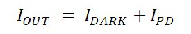
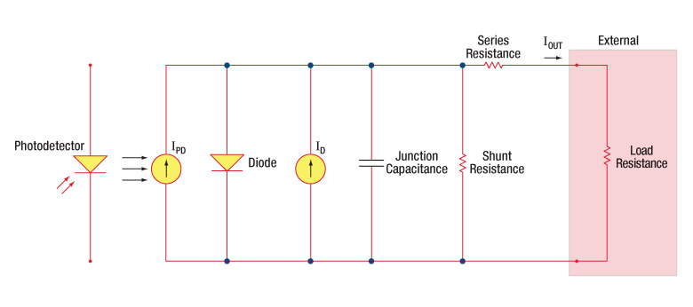
Figure 100A Photodiode Model
Photodiode Terminology
Responsivity
The responsivity of a photodiode can be defined as a ratio of generated photocurrent (IPD) to the incident light power (P) at a given wavelength:
Modes of Operation (Photoconductive vs. Photovoltaic)
A photodiode can be operated in one of two modes: photoconductive (reverse bias) or photovoltaic (zero-bias). Mode selection depends upon the application's speed requirements and the amount of tolerable dark current (leakage current).
Photoconductive
In photoconductive mode, an external reverse bias is applied, which is the basis for our DET series detectors. The current measured through the circuit indicates illumination of the device; the measured output current is linearly proportional to the input optical power. Applying a reverse bias increases the width of the depletion junction producing an increased responsivity with a decrease in junction capacitance and produces a very linear response. Operating under these conditions does tend to produce a larger dark current, but this can be limited based upon the photodiode material. (Note: Our DET detectors are reverse biased and cannot be operated under a forward bias.)
Photovoltaic
In photovoltaic mode the photodiode is zero biased. The flow of current out of the device is restricted and a voltage builds up. This mode of operation exploits the photovoltaic effect, which is the basis for solar cells. The amount of dark current is kept at a minimum when operating in photovoltaic mode.
Dark Current
Dark current is leakage current that flows when a bias voltage is applied to a photodiode. When operating in a photoconductive mode, there tends to be a higher dark current that varies directly with temperature. Dark current approximately doubles for every 10 °C increase in temperature, and shunt resistance tends to double for every 6 °C rise. Of course, applying a higher bias will decrease the junction capacitance but will increase the amount of dark current present.
The dark current present is also affected by the photodiode material and the size of the active area. Silicon devices generally produce low dark current compared to germanium devices which have high dark currents. Table 100B lists several photodiode materials and their relative dark currents, speeds, spectral ranges, and costs.
| Table 100B Photodiode Materials | ||||
|---|---|---|---|---|
| Material | Dark Current | Speed | Spectral Range | Cost |
| Silicon (Si) | Low | High Speed | Visible to NIR | Low |
| Black Silicon (B-Si) | Low | Medium Speeda | Visible to NIR | Moderate |
| Germanium (Ge) | High | Low Speed | NIR | Low |
| Indium Gallium Arsenide (InGaAs) | Low | High Speed | NIR | Moderate |
| Indium Arsenide Antimonide (InAsSb) | High | Low Speed | NIR to MIR | High |
| Extended Range Indium Gallium Arsenide (InGaAs) | High | High Speed | NIR | High |
| Mercury Cadmium Telluride (MCT, HgCdTe) | High | Low Speed | NIR to MIR | High |
Junction Capacitance
Junction capacitance (Cj) is an important property of a photodiode as this can have a profound impact on the photodiode's bandwidth and response. It should be noted that larger diode areas encompass a greater junction volume with increased charge capacity. In a reverse bias application, the depletion width of the junction is increased, thus effectively reducing the junction capacitance and increasing the response speed.
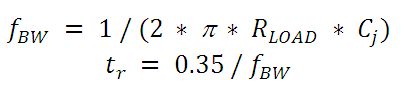
Bandwidth and Response
A load resistor will react with the photodetector junction capacitance to limit the bandwidth. For best frequency response, a 50 Ω terminator should be used in conjunction with a 50 Ω coaxial cable. The bandwidth (fBW) and the rise time response (tr) can be approximated using the junction capacitance (Cj) and the load resistance (RLOAD):
Noise Equivalent Power
The noise equivalent power (NEP) is the input signal power that results in a signal-to-noise ratio (SNR) of 1 in a 1 Hz output bandwidth. This is useful, as the NEP determines the ability of the detector to detect low level light. In general, the NEP increases with the active area of the detector and is given by the following equation:
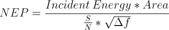
Here, S/N is the Signal to Noise Ratio, Δf is the Noise Bandwidth, and Incident Energy has units of W/cm2. For more information on NEP, please see Thorlabs' Noise Equivalent Power White Paper.
Terminating Resistance
A load resistance is used to convert the generated photocurrent into a voltage (VOUT) for viewing on an oscilloscope:
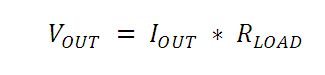
Depending on the type of the photodiode, load resistance can affect the response speed. For maximum bandwidth, we recommend using a 50 Ω coaxial cable with a 50 Ω terminating resistor at the opposite end of the cable. This will minimize ringing by matching the cable with its characteristic impedance. If bandwidth is not important, you may increase the amount of voltage for a given light level by increasing RLOAD. In an unmatched termination, the length of the coaxial cable can have a profound impact on the response, so it is recommended to keep the cable as short as possible.
Shunt Resistance
Shunt resistance represents the resistance of the zero-biased photodiode junction. An ideal photodiode will have an infinite shunt resistance, but actual values may range from the order of ten Ω to thousands of MΩ and is dependent on the photodiode material. For example, and InGaAs detector has a shunt resistance on the order of 10 MΩ while a Ge detector is in the kΩ range. This can significantly impact the noise current on the photodiode. For most applications, however, the high resistance produces little effect and can be ignored.
Series Resistance
Series resistance is the resistance of the semiconductor material, and this low resistance can generally be ignored. The series resistance arises from the contacts and the wire bonds of the photodiode and is used to mainly determine the linearity of the photodiode under zero bias conditions.
Common Operating Circuits
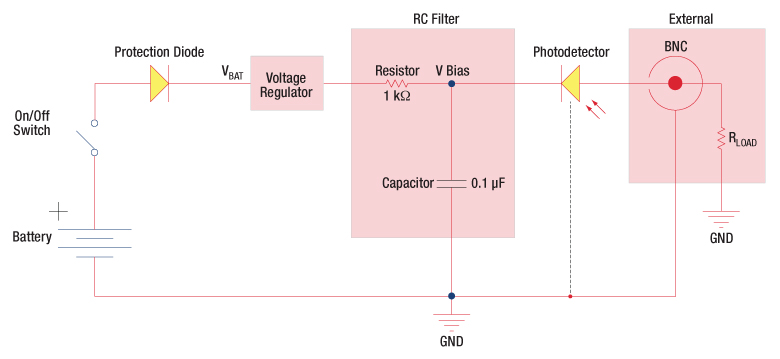
Figure 100C Reverse-Biased Circuit (DET Series Detectors)
The DET series detectors are modeled with the circuit depicted in Figure 100C. The detector is reverse biased to produce a linear response to the applied input light. The amount of photocurrent generated is based upon the incident light and wavelength and can be viewed on an oscilloscope by attaching a load resistance on the output. The function of the RC filter is to filter any high-frequency noise from the input supply that may contribute to a noisy output.
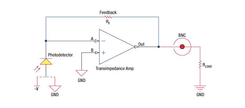
Figure 100D Amplified Detector Circuit
One can also use a photodetector with an amplifier for the purpose of achieving high gain. The user can choose whether to operate in Photovoltaic of Photoconductive modes. There are a few benefits of choosing this active circuit:
- Photovoltaic mode: The circuit is held at zero volts across the photodiode, since point A is held at the same potential as point B by the operational amplifier. This eliminates the possibility of dark current.
- Photoconductive mode: The photodiode is reversed biased, thus improving the bandwidth while lowering the junction capacitance. The gain of the detector is dependent on the feedback element (Rf). The bandwidth of the detector can be calculated using the following:
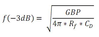
where GBP is the amplifier gain bandwidth product and CD is the sum of the junction capacitance and amplifier capacitance.
Effects of Chopping Frequency
The photoconductor signal will remain constant up to the time constant response limit. Many detectors, including PbS, PbSe, HgCdTe (MCT), and InAsSb, have a typical 1/f noise spectrum (i.e., the noise decreases as chopping frequency increases), which has a profound impact on the time constant at lower frequencies.
The detector will exhibit lower responsivity at lower chopping frequencies. Frequency response and detectivity are maximized for
![]()
The following table lists Thorlab's selection of previous and current generation PDA, PDF, and DET detectors.
| Previous Generation Cross Reference of PDA and DET Detectors | |||||
|---|---|---|---|---|---|
| Wavelength | Material | Biased Detector |
Amplified Detector |
||
| Current Generation | Previous Generation | Current Generation | Previous Generation | ||
| 150 - 550 nm | GaP | DET25K2 | DET25K(/M) | PDA25K2 | PDA25K(-EC) |
| 200 - 1100 nm | Si | DET10A2 | DET10A(/M) | PDA10A2 | PDA10A(-EC) |
| 320 - 1000 nm | Si | - | - | PDA8A2 | PDA8A |
| 320 - 1100 nm | Si | DET100A2 | DET100A(/M)a | PDA100A2 | PDA100A(-EC)b |
| Si | - | - | PDF10A2 | PDF10A(/M) | |
| 350 - 1100 nm | Si | DET36A2 | DET36A(/M) | PDA36A2 | PDA36A(-EC) |
| 500 - 1700 nm | InGaAs | DET10N2 | DET10N(/M) | - | - |
| 800 - 1700 nm | InGaAs | DET20C2 | DET20C(/M) | PDA20CS2 | PDA20CS(-EC) |
| - | - | PDA05CF2 | PDA10CF(-EC) | ||
| - | - | PDA20C2 | PDA20C(/M) | ||
| 800 - 1800 nm | Ge | DET30B2 | DET30B(/M) | PDA30B2 | PDA30B(-EC) |
| DET50B2 | DET50B(/M) | PDA50B2 | PDA50B(-EC) | ||
| 900 - 1700 nm | InGaAs | DET10C2 | DET10C(/M) | PDA10CS2 | PDA10CS(-EC) |
| 900 - 2600 nm | InGaAs | DET05D2 | DET05D(/M)c | PDA10D2 | PDA10D(-EC)c |
| DET10D2 | DET10D(/M)c | - | - | ||
Pulsed Laser Emission: Power and Energy Calculations

Determining whether emission from a pulsed laser is compatible with a device or application can require referencing parameters that are not supplied by the laser's manufacturer. When this is the case, the necessary parameters can typically be calculated from the available information. Calculating peak pulse power, average power, pulse energy, and related parameters can be necessary to achieve desired outcomes including:
- Protecting biological samples from harm.
- Measuring the pulsed laser emission without damaging photodetectors and other sensors.
- Exciting fluorescence and non-linear effects in materials.
Pulsed laser radiation parameters are illustrated in Figure 1 and described in the table. For quick reference, a list of equations are provided below. The document available for download provides this information, as well as an introduction to pulsed laser emission, an overview of relationships among the different parameters, and guidance for applying the calculations.
|
Equations: |
||||
 |
and |  |
||
 |
||||
 |
||||
 |
||||
Peak power and average power calculated from each other: |
||||
 |
and |  |
||
| Peak power calculated from average power and duty cycle*: | ||||
 |
*Duty cycle ( ) is the fraction of time during which there is laser pulse emission. ) is the fraction of time during which there is laser pulse emission. |
|||

Click to Enlarge
Figure 1: Parameters used to describe pulsed laser emission are indicated in the plot (above) and described in the table (below). Pulse energy (E) is the shaded area under the pulse curve. Pulse energy is, equivalently, the area of the diagonally hashed region.
| Parameter | Symbol | Units | Description | ||
|---|---|---|---|---|---|
| Pulse Energy | E | Joules [J] | A measure of one pulse's total emission, which is the only light emitted by the laser over the entire period. The pulse energy equals the shaded area, which is equivalent to the area covered by diagonal hash marks. | ||
| Period | Δt | Seconds [s] | The amount of time between the start of one pulse and the start of the next. | ||
| Average Power | Pavg | Watts [W] | The height on the optical power axis, if the energy emitted by the pulse were uniformly spread over the entire period. | ||
| Instantaneous Power | P | Watts [W] | The optical power at a single, specific point in time. | ||
| Peak Power | Ppeak | Watts [W] | The maximum instantaneous optical power output by the laser. | ||
| Pulse Width |  |
Seconds [s] | A measure of the time between the beginning and end of the pulse, typically based on the full width half maximum (FWHM) of the pulse shape. Also called pulse duration. | ||
| Repetition Rate | frep | Hertz [Hz] | The frequency with which pulses are emitted. Equal to the reciprocal of the period. | ||
Example Calculation:
Is it safe to use a detector with a specified maximum peak optical input power of 75 mW to measure the following pulsed laser emission?
- Average Power: 1 mW
- Repetition Rate: 85 MHz
- Pulse Width: 10 fs
The energy per pulse:

seems low, but the peak pulse power is:

It is not safe to use the detector to measure this pulsed laser emission, since the peak power of the pulses is >5 orders of magnitude higher than the detector's maximum peak optical input power.
| Posted Comments: | |
NorbetTip NorbetTipVH
(posted 2022-02-06 03:36:44.17) Hyosub Kim
(posted 2020-09-09 13:40:15.54) Hi, do you have data about temperature vs. quantum efficiency? asundararaj
(posted 2020-09-17 04:18:17.0) Thank you for contacting Thorlabs. While we do not have the specific temperature dependent data for the PDA50B2, I have contacted you with the general trend one would expect for a Ge photodiodes. Yazhou Wang
(posted 2020-06-12 08:40:50.69) Hi, I saw all the photodetectors can be divided into two kinds, i.e. free space coupling and fiber coupling. What's their difference? Could I use a fiber coupling detector to detect a free space laser beam by focusing the laser beam correctly with some lenses? Can I manually change the fiber coupling detector to free space coupling by revising some of its structure? Thanks. YLohia
(posted 2020-06-12 09:15:52.0) Hello, thank you for contacting Thorlabs. The difference between the two kinds is in the preferred method of delivery of light to the photodiode. One advantage of fiber-coupled detectors is that they can help cut out ambient light from your signal. Fiber-coupled detectors are also sometimes used when the active sensor area is very small. Free space detectors may have larger sensor areas so you would have the ability to use larger beams. You can certainly use a fiber-coupled detector for a free-space beam, but you will lose some power during the fiber coupling process. You can convert a free-space detector to a fiber-coupled one by using one of the threaded adapters for fiber connectors listed on this page. Tariq Shamim Khwaja
(posted 2019-10-08 13:54:28.33) What is the maximum input power density (damage threshold) for PDA50B2? nbayconich
(posted 2019-10-08 11:10:34.0) Thank you for contacting Thorlabs. We do not have an estimated laser induced damage threshold value for these detectors however we recommend that the output current never exceeds 100mA, which could result in damage of the device. The detector should also not be saturated, to avoid this please make sure that the output voltage is between 0-10 volts if using a High impedance termination or 0-5 volts if using a 50ohm termination. The amount of power needed to saturate the detector will depend on the gain setting set on the amplifier and can be calculated using the given transimpedance gain values for each setting. I will reach out to you directly to discuss your application. G A
(posted 2019-07-18 11:37:16.647) Dear Support,
Do you have information about the linearity of the PDA50B2 detector? How does it depends on the wavelength?
Best,
GA asundararaj
(posted 2019-07-22 02:30:23.0) Thank you for contacting Thorlabs. As long as the detector is not saturated and the signal is above the noise floor, the incident power and the photocurrent should have a linear relationship. However, the scale factor of the linearity would depend on the responsivity of the detector, which is wavelength dependent. You can find the responsivity of the detector in the table below. Please note that this is the typical responsivity and will vary from diode to diode. caliari.italo
(posted 2018-10-22 21:26:19.4) could the output signal cable be substituted by a simple 5cm wire with a resistor? YLohia
(posted 2018-10-23 09:44:02.0) This should be fine in terms of measuring a signal, but given that the wire is not coaxial, your signal may have a significant amount of noise. Also, please note that this cannot be accomplished by a single wire -- you will need two (one for a reference ground). We recommend looking into the T3788 BNC to test clips adapter for ease of use. sam.weckx
(posted 2017-12-18 14:33:35.803) Dear,
We consider the installation of a PDA50B amplified photodetector in our application. It would be installed in a vacuum chamber. Can this photodector be installed in a vacuum? Are there other amplified photodectors of thorlabs that can be installed on a vacuum?
Many thanks in advance,
Best regards,
Sam tfrisch
(posted 2018-03-20 03:39:29.0) Hello, thank you for contacting Thorlabs. Unfortunately, these amplified detectors are not suitable for vacuum applications as many components could outgas. jjurado
(posted 2011-02-16 09:24:00.0) Response from Javier at Thorlabs to daniel.grodensky: Thank you very much for contacting us with your request. The dark state noise level is specified to be below -80dBm, measured with "span 5MHz, 3kHz resolution" which refers to the settings of the RF analyzer when measuring the frequency spectrum of the output of the detector under dark conditions (i.e. optical input blocked from light). In this setting, you will find the noise floor to be below -80dBm, which corresponds to 22.5µV RMS in a 50-Ohm system. Taking into account the 3kHz span, this corresponds to a noise level of 0.41µV/sqrt(Hz), or 1.6pW/sqrt(Hz) at the input.
We specify the -80dBm as the maximum noise floor over the whole frequency range; usually the APD210 performs much better than that, down to -92dBm, which actually corresponds to the specified calculated NEP of 0.4pW/sqrt(Hz). daniel.grodensky
(posted 2011-02-08 10:04:07.0) I am interested in APD210, but have a question: What are the full conditions for your dark state noise level (-80dBm = 10pW), or more exactly whats the specified bandwidth? For better of my understanding, having NEP of 0.4pW/sqrHz means that at 1GHz bandwidth the NEP is 12.6nW or -49dBm, the number that 3 orders higher than dark state noise level. Thanks a lot in advance Javier
(posted 2010-06-16 11:21:10.0) Response from Javier at Thorlabs to last poster: the gain adjustment of the APD210 and APD310 detectors controls the APD bias voltage by means of a digital potentiometer that is essentially a resistor network with 100 discrete steps. So, for the APD210, for example, which has a maximum gain of 2.5x10^5 V/W (at 1 GHz, 800 nm), each gain step consists of ~2500 V/W. user
(posted 2010-06-16 10:26:55.0) Hi, What is the minimum gain for APD210 and APD310, also Gain [V/W] at each step? apalmentieri
(posted 2009-12-28 14:41:00.0) A response from Adam at Thorlabs: The APD210 and APD310 have frequency ranges of 1-1600Mhz(APD210) and 1-1800MHz(APD310) respectively. Please note that the 1000MHz listed in the item description refers to the 3dB bandwidth, which is 5-1000MHz for both the APD310 and APD210. user
(posted 2009-12-28 04:18:45.0) Item description says 1000MHz, I dont think that is correct yue77
(posted 2009-09-25 05:30:07.0) Dear team. I am interested in APD210, but have two questions:
1. What are the full conditions for your dark state noise level?
2. How did you calculate NEP, could you provide the necessary parameters?
Thanks a lot in advance. klee
(posted 2009-07-10 21:16:12.0) A response from Ken at Thorlabs to Mattias.Heinrich: Yes, you can use a fiber with these detectors and SM05SMA is the correct adapter if you your fiber is terminated with SMA connector. We also have SM05FC and SM05ST for FC/PC and ST connectors. Mattias.Heinrich
(posted 2009-07-10 11:19:23.0) Hi. Is it possible to couple the detector to a fiber using e.g. the SM05SMA fiber adapter or which other positioning/alignment would you recommend. Thanks in advance. Tyler
(posted 2008-07-23 16:21:35.0) A response from Tyler at Thorlabs to ennui3: Quantum efficiency is defined as the ratio of the number of electrons excited into the conduction band divided by the number of photons absorbed. The QE varies from 0 to an ideal maximum of 1 in standard photodiodes. Since the APD210 is an avalanche photodiode a single photon can potentially generate many conduction electrons and as a result I do not think that the QE is the best measure to be used with this device. With a standard photodiode you can calculate the QE from the responsivity (A/W).
QE=(Rhc)/(le)
Where R is the responsivity in (A/W), h is Planck’s constant, c is the speed of light, l is the wavelength of the light, and e is the magnitude of the charge of an electron.
Thank you for your interest in the APD210 and if you have further questions please post them or contact one of our application engineers. ennui3
(posted 2008-07-18 03:00:27.0) dear.
I want to know the quantumn efficiency of this product.
especially. I want to know Q.E. of wave length at 650nm~750nm.
Does the photo sensitivity mean the Q.E.?
thank you for reading this letter. |
The following table lists Thorlabs' selection of photodiodes, photoconductive, and pyroelectric detectors. Item numbers in the same row contain the same detector element.
| Photodetector Cross Reference | ||||||
|---|---|---|---|---|---|---|
| Wavelength | Material | Unmounted Photodiode |
Mounted Photodiode |
Biased Detector |
Amplified Detector |
Amplified Detector, OEM Package |
| 200 - 1100 nm | Si | FDS010 | SM05PD2A SM05PD2B |
DET10A2 | PDA10A2 | PDAPC5 |
| Si | - | SM1PD2A | - | - | - | |
| 240 - 1170 nm | Black Si | FDBS11 | SM05PD9A | - | - | - |
| Black Si | FDBS22 | SM05PD8A | DET20X2 | PDA20X2 | PDAPC10 | |
| Black Si | FDBS25 | - | - | - | - | |
| 320 - 1000 nm | Si | - | - | - | PDA8A2 | - |
| 320 - 1100 nm | Si | FD11A | SM05PD3A | - | PDF10A2 | - |
| Si | - a | - | DET100A2 a | PDA100A2 a | PDAPC2 a | |
| 340 - 1100 nm | Si | FDS10X10 | - | - | - | - |
| 350 - 1100 nm | Si | FDS100 FDS100-CAL b |
SM05PD1A SM05PD1B |
DET36A2 | PDA36A2 | PDAPC1 |
| Si | FDS1010 FDS1010-CAL b |
SM1PD1A SM1PD1B |
- | - | - | |
| 400 - 1000 nm | Si | - | - | - | PDA015A2 FPD310-FS-VIS FPD310-FC-VIS FPD510-FC-VIS FPD510-FS-VIS FPD610-FC-VIS FPD610-FS-VIS |
- |
| 400 - 1100 nm | Si | FDS015 c | - | - | - | - |
| Si | FDS025 c FDS02 d |
- | DET02AFC ( /M ) DET025AFC ( /M ) DET025A ( /M ) DET025AL ( /M ) |
- | - | |
| 400 - 1700 nm | Si & InGaAs | DSD2 | - | - | - | - |
| 500 - 1700 nm | InGaAs | - | - | DET10N2 | - | - |
| 0.6 - 16 µm | LiTaO 3 | - | - | - | PDA13L2 e | - |
| 750 - 1650 nm | InGaAs | - | - | - | PDA8GS | - |
| 800 - 1700 nm | InGaAs | FGA015 | - | - | PDA015C2 | - |
| InGaAs | FGA21 FGA21-CAL b |
SM05PD5A | DET20C2 | PDA20C2 PDA20CS2 |
- | |
| InGaAs | FGA01 c FGA01FC d |
- | DET01CFC ( /M ) | - | - | |
| InGaAs | FDGA05 c | - | - | PDA05CF2 | PDAPC6 | |
| InGaAs | - | - | DET08CFC ( /M ) DET08C ( /M ) DET08CL ( /M ) |
- | - | |
| InGaAs | - | - | - | PDF10C2 | - | |
| 800 - 1800 nm | Ge | FDG03 FDG03-CAL b |
SM05PD6A | DET30B2 | PDA30B2 | - |
| Ge | FDG50 | - | DET50B2 | PDA50B2 | PDAPC8 | |
| Ge | FDG05 | - | - | - | - | |
| 900 - 1700 nm | InGaAs | FGA10 | SM05PD4A | DET10C2 | PDA10CS2 | - |
| 900 - 2600 nm | InGaAs | FD05D | - | DET05D2 | - | - |
| FD10D | - | DET10D2 | PDA10D2 | PDAPC7 | ||
| 950 - 1650 nm | InGaAs | - | - | - | FPD310-FC-NIR FPD310-FS-NIR FPD510-FC-NIR FPD510-FS-NIR FPD610-FC-NIR FPD610-FS-NIR |
- |
| 1.0 - 5.8 µm | InAsSb | - | - | - | PDA10PT ( -EC ) | - |
| 2.0 - 8.0 µm | HgCdTe (MCT) | VML8T0 VML8T4 f |
- | - | PDAVJ8 | - |
| 2.0 - 10.6 µm | HgCdTe (MCT) | VML10T0 VML10T4 f |
- | - | PDAVJ10 | - |
| 2.7 - 5.0 µm | HgCdTe (MCT) | VL5T0 | - | - | PDAVJ5 | - |
| 2.7 - 5.3 µm | InAsSb | - | - | - | PDA07P2 | PDAPC9 |
| Item #a | Housing Featuresb | Wavelength Range |
Bandwidth Range | NEPc | Responsivity Data |
Active Aread,e | Operating Temperature Range |
Power Supply Included |
|---|---|---|---|---|---|---|---|---|
| PDA50B2 |  |
800 - 1800 nm | DC - 510 kHz | 4.63 x 10⁻¹² to 1.76 x 10⁻¹⁰ W/Hz1/2 |
Click Here for Raw Data |
19.6 mm2 (Ø5.0 mm) |
10 to 40 °C | Yes |
| PDA30B2 |  |
800 - 1800 nm | DC - 590 kHz | 5.93 x 10⁻¹² to 1.44 x 10⁻¹⁰ W/Hz1/2 |
Click Here for Raw Data |
7.1 mm2 (Ø3.0 mm) |
10 to 40 °C | Yes |

 Zoom
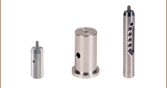
ZoomMale Connector on Cable
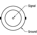
The PDA-C-72 power cord is offered for the PDA line of amplified photodetectors when using with a power supply other than the one included with the detector. The cord has tinned leads on one end and a PDA-compatible 3-pin connector on the other end. It can be used to power the PDA series of amplified photodetectors with any power supply that provides a DC voltage. The pin descriptions are shown to the right.

 Zoom
Zoom
LDS12B Male Power Cable
- Replacement Power Supply for the PDA and PDF Amplified Photodetectors Sold Above
- ±12 VDC Power Output
- Current Limit Enabling Short Circuit and Overload Protection
- On/Off Switch with LED Indicator
- Switchable AC Input Voltage (100, 120, or 230 VAC)
- 2 m (6.6') Cable with LUMBERG RSMV3 Male Connector
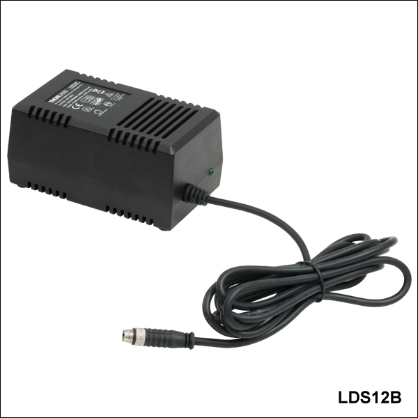
- UL and CE Compliant
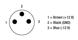
The LDS12B ±12 VDC Regulated Linear Power Supply is intended as a replacement for the supply that comes with our PDA and PDF line of amplified photodetectors sold on this page. The cord has three pins: one for ground, one for +12 V, and one for -12 V (see diagram to the right). A region-specific power cord is shipped with the unit based on your location. This power supply can also be used with the PDB series of balanced photodetectors, PMM series of photomultiplier modules,APD series of avalanche photodetectors, and the FSAC autocorrelator for femtosecond lasers.
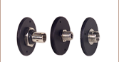
- FC/APC (Narrow Key or Wide Key), SMA, ST®*/PC, SC/PC, or LC/PC Fiber Receptacles.
- Light-Tight Construction When Used with SM1 Lens Tubes
- Compatible with Many of Our Photodiode Power Sensors
Note: The APC adapters have two dimples in the front surface that allow them to be tightened with the SPW909 or SPW801 spanner wrench. The dimples do not go all the way through the disk so that the adapter can be used in light-tight applications when paired with SM1 lens tubes.
FC/APC adapters are available with either narrow (2.0 mm) or wide (2.2 mm) key connectors; for more details on narrow versus wide key connectors, please see our Intro to Fiber tutorial.
| Item # | S120-APC2a | S120-APCa | S120-SMA | S120-ST | S120-SC | S120-LC |
|---|---|---|---|---|---|---|
| Adapter Image (Click the Image to Enlarge) |
 |
 |
 |
 |
 |
 |
| Fiber Connector Type | FC/APC, 2.0 mm Narrow Key |
FC/APC 2.2 mm Wide Key |
SMA | ST/PC | SC/PCb | LC/PC |
| Threading | Internal SM1 (1.035"-40) | |||||
*ST® is a registered trademark of Lucent Technologies, Inc.
- FC/PC (Narrow or Wide Key), FC/APC (Narrow or Wide Key), SMA, ST®*/PC, SC/PC, or LC/PC Receptacles
- Vacuum-Compatible Versions of FC/PC Wide-Key and SMA Receptacles Available
- Light-Tight When Used with SM1 Lens Tubes
- Compatible with Many of Our 30 mm Cage Plates and Photodetectors
Note: Each disk has four dimples, two in the front surface and two in the back surface, that allow it to be tightened from either side with the SPW909 or SPW801 spanner wrench. The dimples do not go all the way through the disk so that the adapters can be used in light-tight applications when paired with SM1 lens tubes. Once the adapter is at the desired position, use an SM1RR retaining ring to secure it in place.
FC/PC and FC/APC adapters are available with either narrow (2.0 mm) or wide (2.2 mm) key connectors; for more details on narrow versus wide key connectors, please see our Intro to Fiber tutorial.
| Item # | SM1FC2 | SM1FC | SM1FCV | SM1FCA2a | SM1FCAa | SM1SMA | SM1SMAV | SM1ST | SM1SC1b | SM1LCb |
|---|---|---|---|---|---|---|---|---|---|---|
| Adapter Image (Click the Image to Enlarge) |
 |
 |
 |
 |
 |
 |
 |
 |
 |
 |
| Connector Type | FC/PC, 2.0 mm Narrow Key |
FC/PC, 2.2 mm Wide Key |
FC/PC, 2.2 mm Wide Key |
FC/APC, 2.0 mm Narrow Key |
FC/APC, 2.2 mm Wide Key |
SMA | SMA | ST/PC | SC/PCc | LC/PC |
| Vacuum Compatibility | - | >10-10 Torr | - | >10-10 Torr | - | |||||
| Threading | External SM1 (1.035"-40) | |||||||||
*ST® is a registered trademark of Lucent Technologies, Inc.