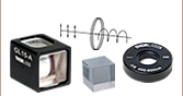
 Products Home
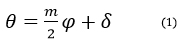
Zero-Order Vortex Half-Wave Retarders

- Radially and Azimuthally Polarize Light from a Linearly Polarized Source
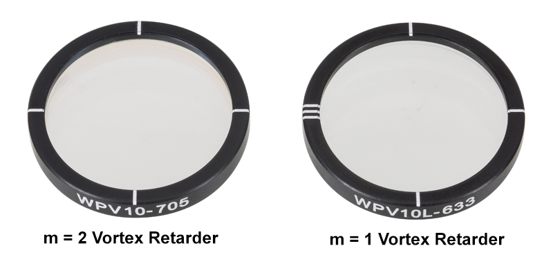
- Available as Either an m = 1 or m = 2 Vortex Retarder
- Create "Donut Hole" Beam Profiles from Gaussian Beams
- Center Wavelengths Available from 532 nm to 1550 nm
WPV10-532
m = 2 Vortex Retarder, 532 nm
WPV10L-780
m = 1 Vortex Retarder, 780 nm
WPV10-1064
m = 2 Vortex Retarder, 1064 nm
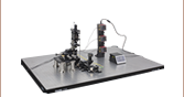
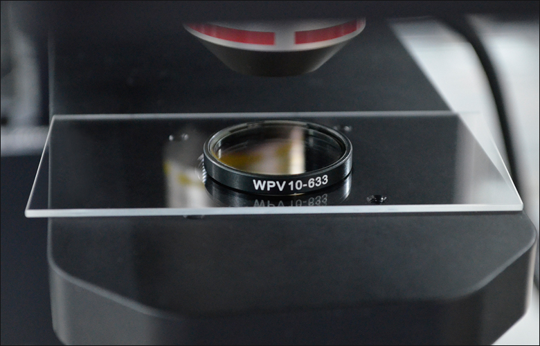
Application Idea
The WPV10-633 Vortex
Retarder Mounted in an
ST1XY-D XY Translation Mount


Please Wait
Click to Enlarge
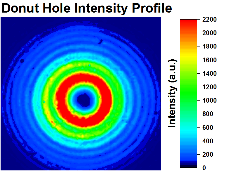
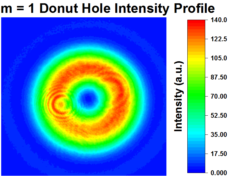
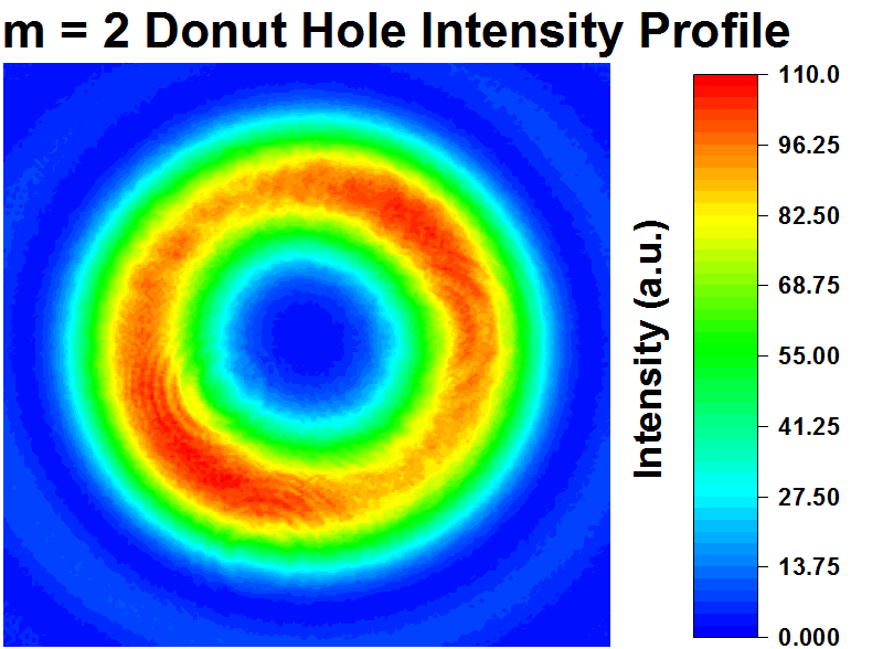
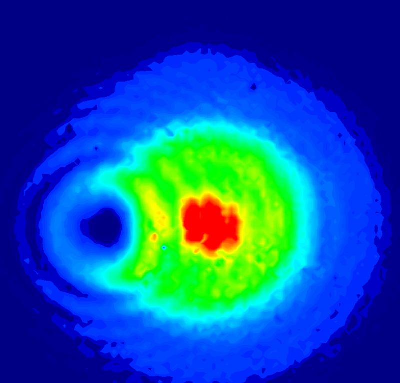
Figure 1.2 The intensity profile of a Laguerre-Gaussian donut hole beam generated by WPV10-532 m = 2 vortex retarder. See the LG Mode & Alignment tab for more information.
Click to Enlarge
Figure 1.1 Each retarder is engraved with its part number and leader lines to aid in alignment.
Features
- True Zero-Order Vortex Half-Wave Plates
- Controls Radial and Azimuthal Polarizations
- Options for m = 1 or m = 2 Vortex Retarder
(See the Comparison Tab) - Center Wavelength Options from 532 nm to 1550 nm
(See Specs Tab) - Compatible with Beam Sizes from Ø300 µm to Ø21.5 mm
- Large AOI of ±20°
- Custom Vortex Retarders Available
Thorlabs’ Liquid Crystal Polymer (LCP) Vortex Retarders are half-wave retarders designed to affect the radial and azimuthal polarization of optical fields. A vortex retarder has a constant retardance across the clear aperture but its fast axis rotates continuously over the area of the optic. These retarders are offered as either m = 1 (Item # Prefix WPV10L) or m = 2 (Item # Prefix WPV10) order vortex retarders. The difference between the two orders is the fast axis distribution over the clear aperture of the retarder. As a result, they generate different polarization patterns from linearly polarized light (see the Comparison tab for more information).
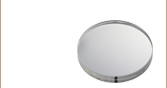
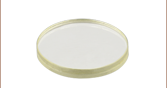
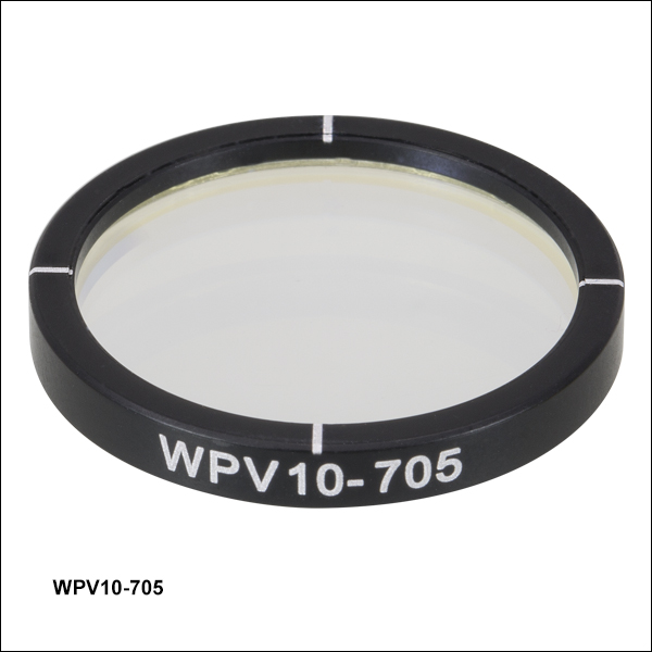
These retarders are mounted in an aluminum housing with an engraving along the perimeter to assist in locating the center point of the plate for beam alignment purposes. The m = 1 retarders have an additional mark, denoted by 3 lines, to indicate the orientation of the zero-degree fast axis (see Figure 1.1). Each LCP vortex retarder is composed of a thin LCP film sandwiched between two Ø23 mm, 1 mm thick N-BK7 glass plates. Photo-alignment techniques set the LCP molecules' orientations to create the continuously rotating fast axis, with the point of rotation at the center of the optic. Due to their construction, these retarders can accept a large AOI of ±20°. Additionally, they are compatible with beam diameters from 21.5 mm (0.84") down to 0.3 mm (0.01").
Vortex retarders convert standard TEM00 Gaussian beams into so-called "donut hole" Laguerre-Gaussian modes, as shown in Figure 1.2. Both the m = 1 and m = 2 retarders are capable of generating a donut hole shaped beam; however, the polarization direction of the resulting beam will be different (see the Comparison tab for more information). In general, the m = 1 retarder will produce a smaller, more circular donut hole compared to the m = 2. Vortex retarders should be used at a single wavelength close to the design wavelength; the donut beam profile will degrade as the deviation from the design wavelength increases.
The point of rotation for the fast axis is nominally located in the center of the glass substrate, but has a Ø1 mm variable range from retarder to retarder. The engraved lines on the housing of these devices give a rough indication as to the position of the center.
An AR coating is applied to both outer surfaces to improve the transmission through the optic at its specified wavelength. They are mounted in a thin walled, Ø1" housing that is compatible with many of our Ø1" optic mounts, including XY translation mounts.
| Vortex Retarder General Specifications | |||||||||||
|---|---|---|---|---|---|---|---|---|---|---|---|
| Item # | WPV10-532 WPV10L-532 |
WPV10-633 WPV10L-633 |
WPV10-705 WLP10L-705 |
WPV10-780 WPV10L-780 |
WPV10-830 WPV10L-830 |
WPV10-980 WPV10L-980 |
WPV10-1064 WPV10L-1064 |
WPV10-1310 WPV10L-1310 |
WPV10-1550 WPV10L-1550 |
||
| Design Wavelength | 532 nm | 633 nm | 705 nm | 780 nm | 830 nm | 980 nm | 1064 nm | 1310 nm | 1550 nm | ||
| Transmission at Design Wavelengtha |
≥97% | ≥97% | ≥97% | ≥97% | ≥97% | ≥97% | ≥96% | ≥96% | ≥96% | ||
| AR Coating Range | 350 - 700 nm | 650 - 1050 nm | 1050 - 1700 nm | ||||||||
| Average Reflectance (per Surface)b |
<0.5% | ||||||||||
| Angle of Incidencec | ±20° | ||||||||||
| Material | Liquid Crystal Polymer Between N-BK7 Glass Plates | ||||||||||
| Retardance | λ/2 | ||||||||||
| Outer Diameter | 25.4 ± 0.2 mm (1.00" ± 0.008") | ||||||||||
| Clear Aperture | Ø21.5 mm (Ø0.85") | ||||||||||
| Housing Thickness | 3.4 mm (0.13") | ||||||||||
| Surface Quality | 60-40 Scratch-Dig | ||||||||||
| Operating Temperature Range | -20 to 60 °C | ||||||||||
| Temperature Stability | <0.08 nm/°C over the Operating Temperature Range | ||||||||||
| Beam Deviation | <20 arcmin | ||||||||||
| Vortex Retarder Order | |||
|---|---|---|---|
| Item # | Order | Item # | Order |
| WPV10L-532 |
m = 1 | WPV10-532 | m = 2 |
| WPV10L-633 |
WPV10-633 | ||
| WPV10L-705 | WPV10-705 | ||
| WPV10L-780 |
WPV10-780 | ||
| WPV10L-830 |
WPV10-830 | ||
| WPV10L-980 |
WPV10-980 | ||
| WPV10L-1064 |
WPV10-1064 | ||
| WPV10L-1310 | WPV10-1310 | ||
| WPV10L-1550 | WPV10-1550 | ||
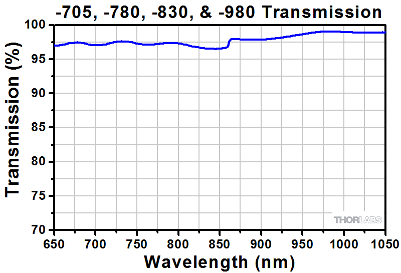
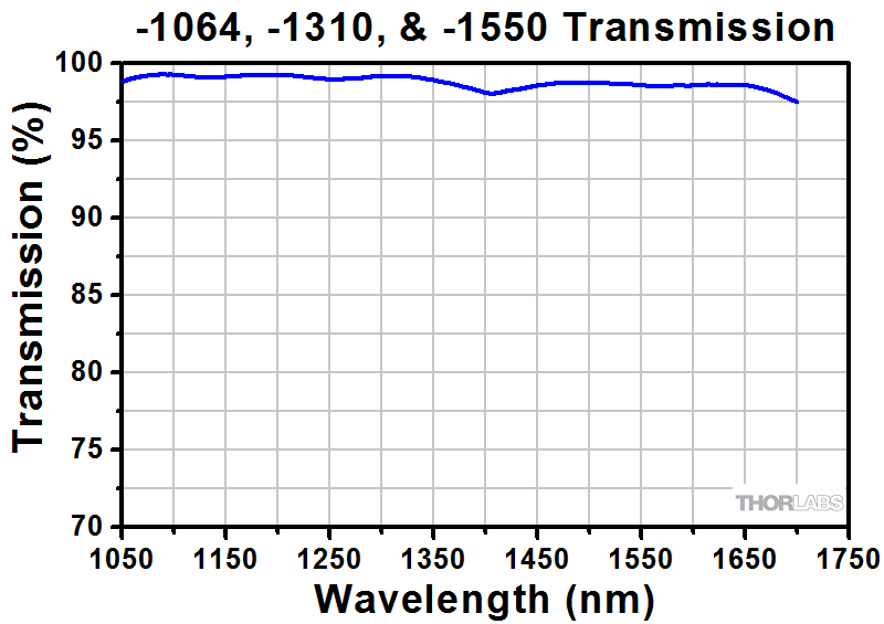
Figures 3.1 through 3.7 are provided as examples of the typical performance of Thorlabs' Vortex Retarders. Actual performance will vary from lot to lot within the specifications provided on the Specs tab.

Click to Enlarge
Figure 3.1 Transmission curve for the WPV10L-532, WPV10L-633, WPV10-532, and WPV10-633 Vortex Retarders. Click here for Raw Data.
Click to Enlarge
Figure 3.2 Transmission curve for WPV10L-705, WPV10L-780, WPV10L-830, WPV10L-980, WPV10-705, WPV10-780, WPV10-830, and WPV10-980 Vortex Retarders. Click here for Raw Data.
Click to Enlarge
Figure 3.3 Transmission curve for the WPV10L-1064, WPV10L-1310, WPV10L-1550, WPV10-1064, WPV10-1310, and WPV10-1550 Vortex Retarders. Click here for Raw Data.
m = 1 Vortex Retarders
Click to Enlarge
Figure 3.4 This plot shows the fast axis orientation over the surface of our m=1 vortex retarders.
The 0° fast axis angle location is indicated by three lines on the retarder's mount.
Click to Enlarge
Figure 3.5 The intensity profile of a Laguerre-Gaussian donut hole beam generated by the WPV10L-633 m = 1 Vortex Retarder.
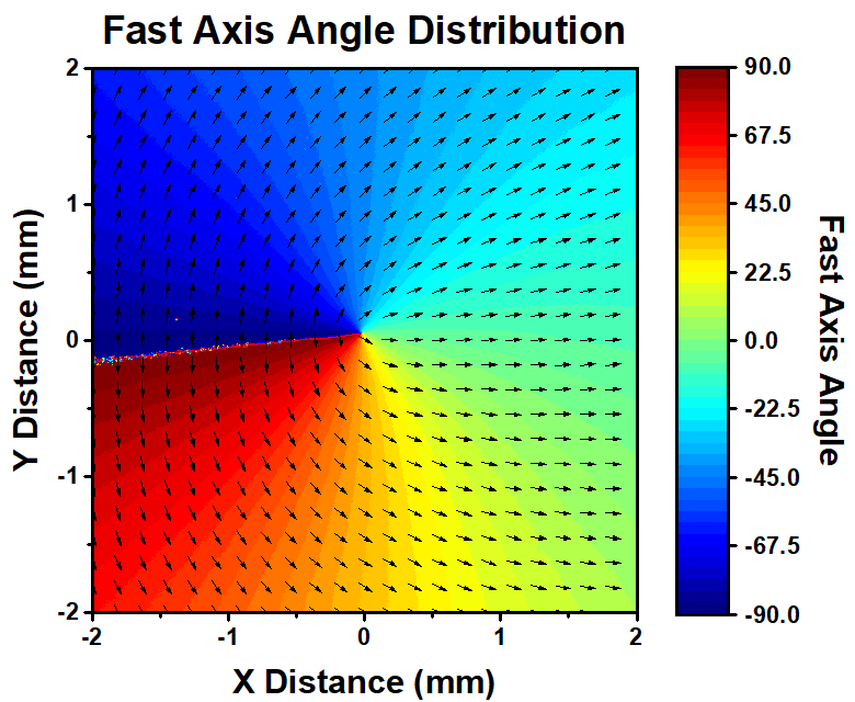
m = 2 Vortex Retarders

Click to Enlarge
Figure 3.6 This plot shows the fast axis orientation over the surface of our m=2 vortex retarders.
Click to Enlarge
Figure 3.7 The intensity profile of a Laguerre-Gaussian donut hole beam generated by the WPV10-633 m = 2 Vortex Retarder.
| Table 4.1 Vortex Retarder Comparison | |||
|---|---|---|---|
| Item Prefix | WPV10L | WPV10 | |
| Order | m = 1 | m = 2 | |
| Generates Donut Beam | Yes | Yes | |
| Relative Donut Hole Shape (Click for Graph) |
Smaller and More Circular | Larger and More Elliptical | |
| Input Polarization Dependent | Yes | No | |
| Output Light Polarization Pattern | m = 2 Vortex Pattern | m = 4 Vortex Pattern | |
Retarder Order
Thorlabs offers both m = 1 and m = 2 vortex wave plates, where m is known as the order as seen in the equation below.
Here θ is the orientation of the fast-axis as a given azimuthal angle (φ) on the waveplate, δ is the orientation of the fast axis at φ = 0. Thus different ordered waveplates will have a different distribution of the fast axis about the center of the device. Figures 4.2 and 4.3 depict the fast axis pattern on our m = 1 and m = 2 retarders, respectively.
Click to Enlarge
Figure 4.3 This plot shows the fast axis orientation (denoted by arrows) over the surface of our m=2 vortex retarders.
Click to Enlarge
Figure 4.2 This plot shows the fast axis orientation (denoted by arrows) over the surface of our m = 1 vortex retarders.
Table 4.1 highlights some of the main differences between the m = 1 and m = 2 vortex retarders, including graphs of the generated donut beams by each style retarder. Both of these intensity profiles were created from the same 633 nm laser source. The profile created by the m = 1 retarder has a smaller central hole (about Ø0.25 mm) than the profile from the m = 2 waveplate (about Ø0.4 mm). Furthermore, the former is more circular than the latter.
Another notable difference is that the m = 2 vortex retarder is a polarization independent device. Due to its fast axis distribution, it will generate similar polarization distributions regardless of the incident polarization direction of the light. The m = 1 retarder is polarization dependent; the waveplate can produce different polarization directions for differing orientations of the retarder to the polarization axis of the light, as seen in Figure 4.4.
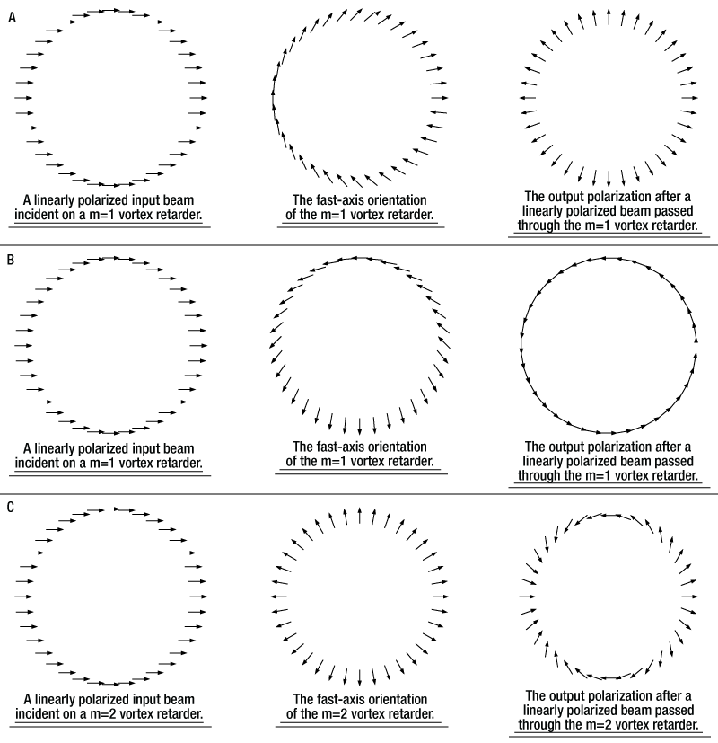
Figure 4.4 Rows A and B show the resulting polarization from a linearly polarized source for an m = 1 vortex retarder. The input polarization is the same, but the relative angle of the fast axis is different, producing different output polarizations. Row C demonstrates the polarization insensitive nature of the m = 2 retarder.
Click to Enlarge
Figure 5.1 The intensity profile of a Laguerre-Gaussian donut hole beam.
Generating Laguerre-Gaussian Donut Hole Laser Modes
Thorlabs makes several versions of these Vortex Retarders to accommodate a range of design wavelengths from 532 nm to 1550 nm (see Specs tab for more information). To generate the Laguerre-Gaussian donut hole laser modes, simply match the design wavelength of the retarder to that of the laser source. A CMOS beam profiler* can be used to measure the resultant laser beam’s intensity distribution. Both our m = 1 and m = 2 retarders are capable of producing a donut hole laser mode.
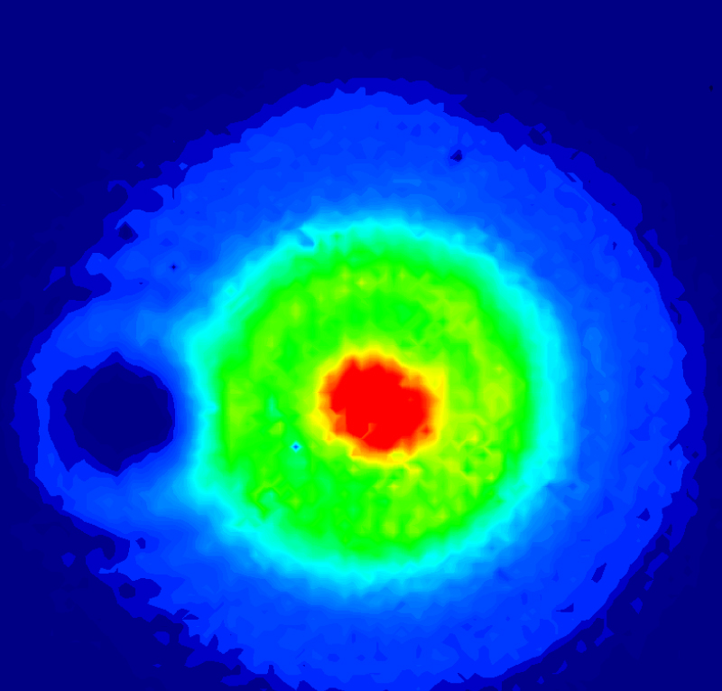
Figure 5.1 shows the donut hole mode generated by the WPV10-532 m = 2 Vortex Retarder aligned with the center of the beam. A 532 nm laser with a Ø0.684 mm beam size was used for this example. The false color plot was captured using the previous-generation
Figures 5.2 through 5.6 show the alignment of this retarder with a laser beam. The point of rotation for the fast axis is nominally located in the center of the glass substrate, but has a Ø1 mm variable range from retarder to retarder. The engraved lines on the housing of these devices gives a rough indication as to the position of the center. A CCD profiler was used to measure the beam shape as the retarder was translated across the beam’s diameter.
*A scanning slit beam profiler should not be used, as these devices calculate the beam shape based on the assumption of a near-Gaussian beam profile.
Click to Enlarge
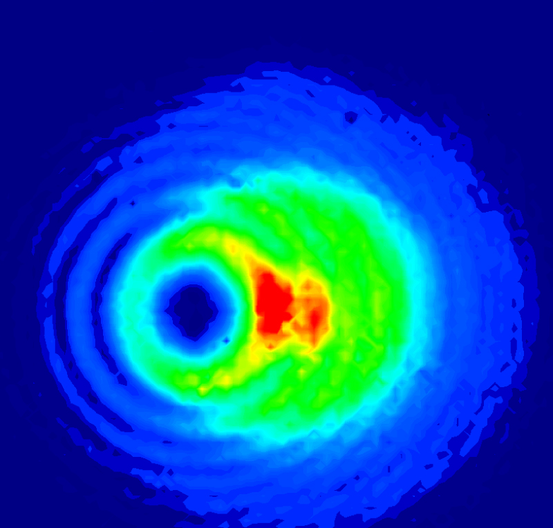
Figure 5.2 Intensity Profile with Laser Beam Off Center of Vortex Retarder by 2.0 mm
Click to Enlarge
Figure 5.3 Intensity Profile with Laser Beam Off Center of Vortex Retarder by 1.5 mm
Click to Enlarge
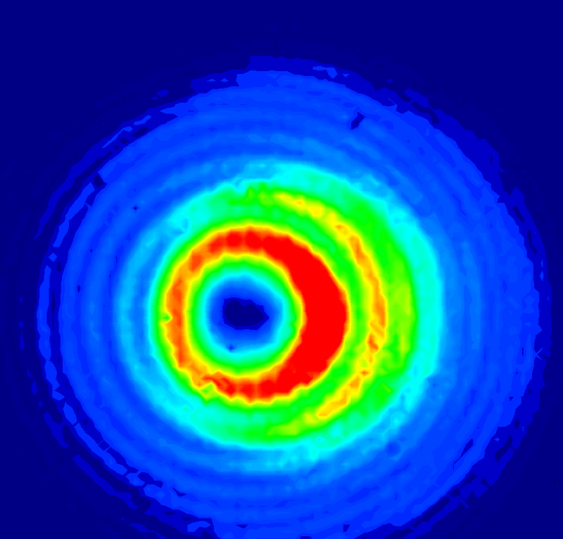
Figure 5.4 Intensity Profile with Laser Beam Off Center of Vortex Retarder by 1.0 mm
Click to Enlarge
Figure 5.5 Intensity Profile with Laser Beam Off Center of Vortex Retarder by 0.5 mm
Click to Enlarge
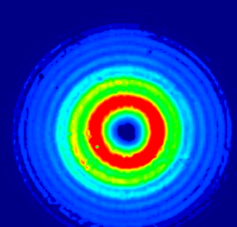
Figure 5.6 Intensity Profile with Laser Beam Centered on Vortex Retarder
Click to Enlarge
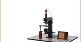
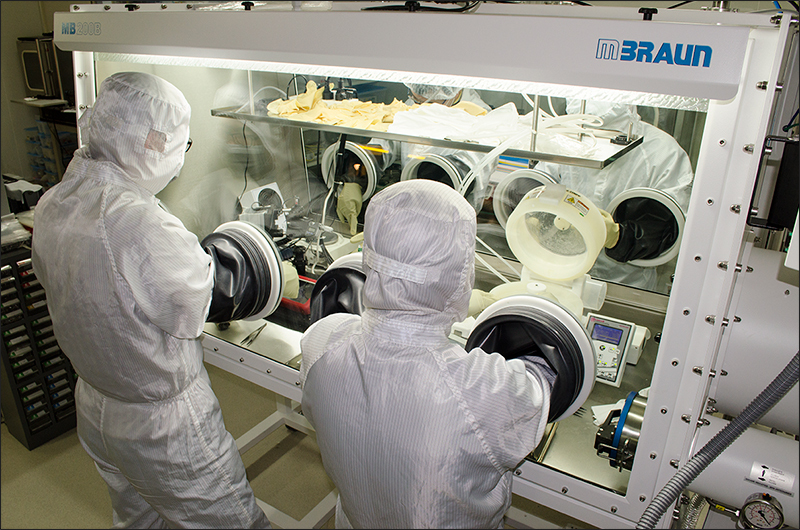
Figure 6.1 Our highly trained engineers constructing and testing polymer vortex retarders.
Thorlabs offers a variety of polymer vortex retarders with operating wavelengths from 532 to 1550 nm, mounted in Ø1" mechanical housings. In addition, we also offer OEM and custom polymer vortex retarders upon request. The target wavelength, order, coating, mechanical housing, and dimensions can all be customized to meet unique optical design requirements.
Our engineers work directly with our customers to discuss the specifications and other design aspects of custom vortex retarders. We analyze both the design and feasibility to ensure the custom products are manufactured to the highest quality standards and in a timely manner. For more information about ordering a custom vortex retarder, please contact Technical Support.
Coating and Fast-Axis Alignment of the Photo-Alignment Material
Vortex retarders utilize a liquid crystal polymer, similar to nematic liquid crystals, which requires the polymer molecules to be aligned. To accomplish this, an alignment layer is created by coating a substrate in photo-alignment material and exposing it to polarized laser light. A 20 to 30 nm layer of photo-alignment material is deposited on a glass substrate by spin coating (see Figure 6.2). The coated substrate is then placed in the photo-alignment system for alignment, where it is rotated at 120 RPM while being exposed to a linearly polarized line of light (width <3 µm, length >25.4 mm). The molecules in the coating align with the polarization axis of the incident line of light. The center of rotation for the substrate is positioned on the light line to minimize center misalignment.
In addition to these vortex retarders, we can also offer a wide variety of stock and custom patterned retarders and wave plates.
Custom Retardance
The retardance of a vortex retarder is determined by the thickness of a layer of cured liquid crystal polymer. This layer is coated on top of the alignment material using a spin coating technique, enabling precise control of the layer's thickness. Our stock vortex retarders cover many commonly used wavelengths. Custom retarders for single wavelengths between 488 and 1550 nm can be special ordered as well.
Custom m Values
The order of a vortex retarder is controlled by a precise photo alignment of the liquid crystal polymer. Our in-house manufacturing capabilities allow us to create custom retarders of higher order (m > 2).
Custom Size and Mounting Options
We offer Ø1" mounted vortex retarders from stock. Custom vortex retarders are available in sizes ranging from Ø0.2" to Ø1" and can be ordered either mounted or unmounted.
Testing
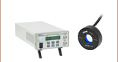
Each vortex retarder is tested for birefringence, uniformity, and fast axis angle. An imaging polarimeter measures the 2-dimensional birefringence distribution across the wave plate's face. Figures 6.3, 6.4, and 6.5 show testing rigs for our polymer wave plates.
Click for Details
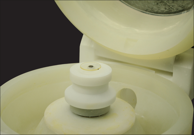
Figure 6.2 A glass substrate mounted on the spin coating machine ready to be coated with the photo alignment material.
Click for Details
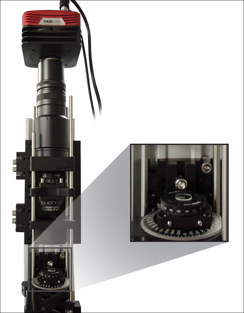
Figure 6.3 The test setup for checking the retardance and alignment uniformity of our vortex retarders.
Click to Enlarge
Figure 6.4 A second test setup for checking the alignment and uniformity of our vortex retarders.
Click to Enlarge
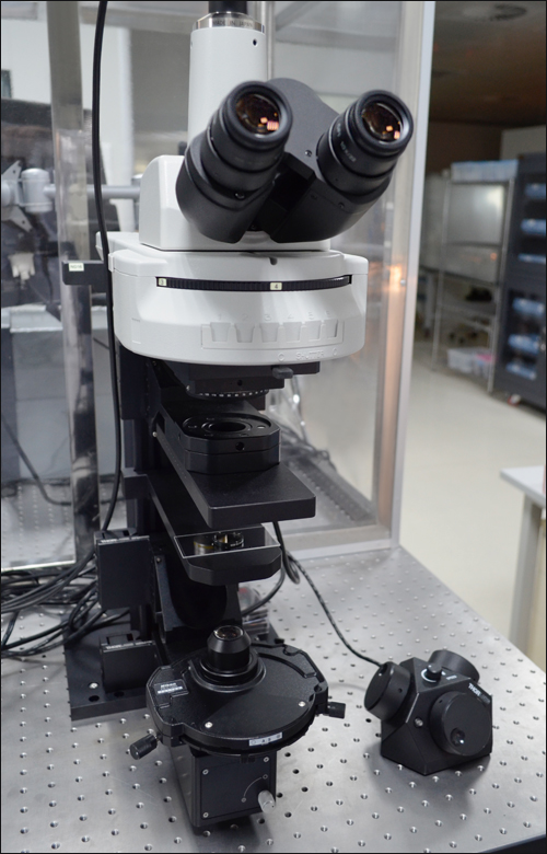
Figure 6.5 A close up of a vortex retarder in one of the test setups.
| Custom Capability | Custom Specification |
|---|---|
| Patterned Retarder Size | Ø100 µm to Ø2" |
| Patterned Retarder Shape | Any |
| Microretarder Size | ≥Ø30 µm |
| Microretarder Shape | Round or Square |
| Retardance Range @ 632.8 nm | 50 to 550 nm |
| Substrate | N-BK7, UV Fused Silica, or Other Glass |
| Substrate Size | Ø5 mm to Ø2" |
| AR Coating | -A: 350 - 700 nm -B: 650 - 1050 nm -C: 1050 - 1700 nm |
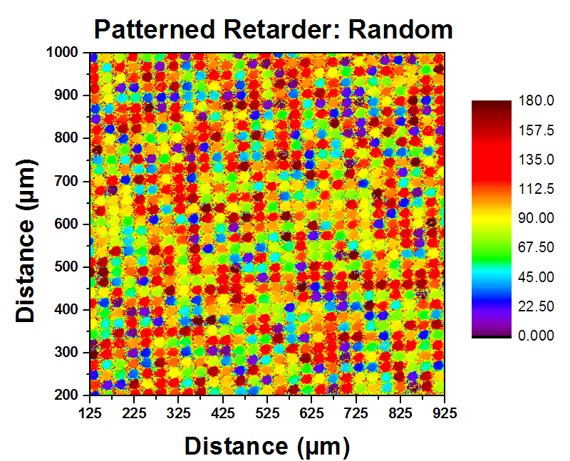
Click to Enlarge
Figure 97A Patterned Retarder with Random Distribution
Features
- Build a Custom Microretarder
- Customize Size, Shape, and Substrate Material
- Retardance Range: 50 - 550 nm
- Fast Axis Resolution: <1º
- Retardance Fluctuations Under 30 nm
Applications
- 3D Displays
- Polarization Imaging
- Diffractive Optical Applications: Polarization Gratings, Polarimetry, and Beam Steering
Thorlabs offers customizable patterned retarders, available in any pattern size from Ø100 µm to Ø2" and any substrate size from Ø5 mm to Ø2". These custom retarders are composed of an array of microretarders, each of which has a fast axis aligned to a different angle than its neighbor. The size and shape of the microretarders are also customizable. They can be as small as 30 µm and in shapes including circles and squares. This control over size and shape of the individual microretarders allows us to construct a large array of various patterned retarders to meet nearly any experimental or device need.
These patterned retarders are constructed from our liquid crystals and liquid crystal polymers. Using photo alignment technology, we can secure the fast axis of each microretarder to any angle within a resolution of <1°. Figures 97A, 97B, and 97C show examples of our patterned retarders. The figures represent measured results of the patterned retarder captured on an imaging polarimeter and demonstrate that the fast axis orientation of any one individual microretarder can be controlled deterministically and separately from its neighbors.
The manufacturing process for our patterned retarders is controlled completely in house. It begins by preparing the substrate, which is typically N-BK7 or UV fused silica (although other glass substrates may be compatible as well). The substrate is then coated with a layer of photoalignment material and placed in our patterned retarder system where sections are exposed to linearly polarized light to set the fast axis of a microretarder. The area of the exposed sections depends on the desired size of the microretarder; the fast axis can be set between 0° and 180° with a resolution <1°. Once set, the liquid crystal cell is constructed by coating the device with a liquid crystal polymer and curing it with UV light.
Thorlabs' LCP depolarizers provide one example of these patterned retarders. In principle, a truly randomized pattern may be used as a depolarizer, since it scrambles the input polarization spatially. However, such a pattern will also introduce a large amount of diffraction. For our depolarizers, we designed a linearly ramping fast axis angle and retardance that can depolarize both broadband and monochromatic beams down to diameters of 0.5 mm without introducing additional diffraction. For more details, see the webpage for our LCP depolarizers.
By supplying Thorlabs with a drawing of the desired patterned retarder or an excel file of the fast axis distribution, we can construct almost any patterned retarder. For more information on creating a patterned retarder, please contact Tech Support.
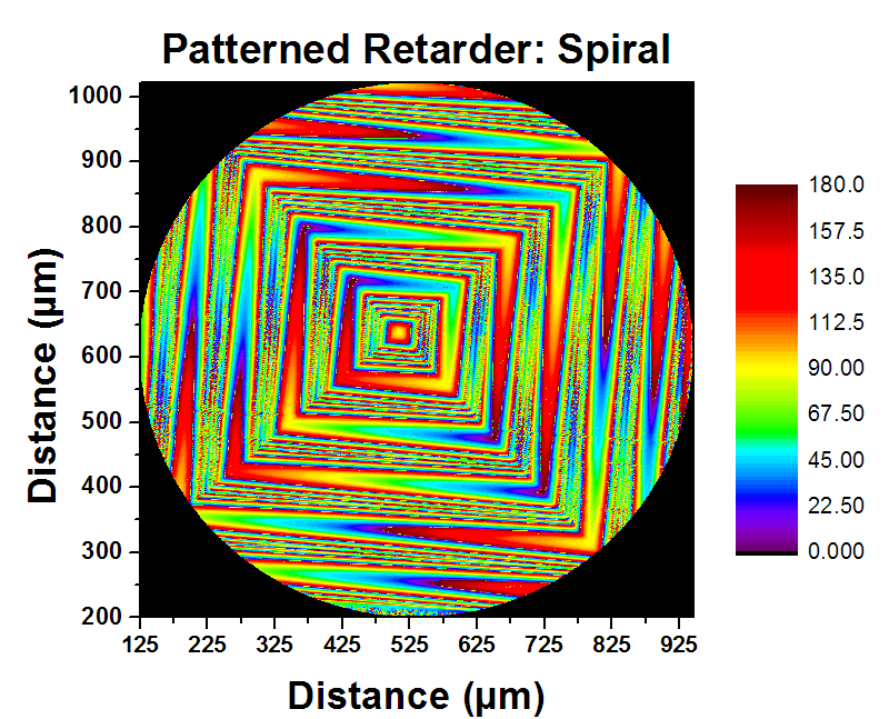
Click to Enlarge
Figure 97B Patterned Retarder with a Spiral Distribution
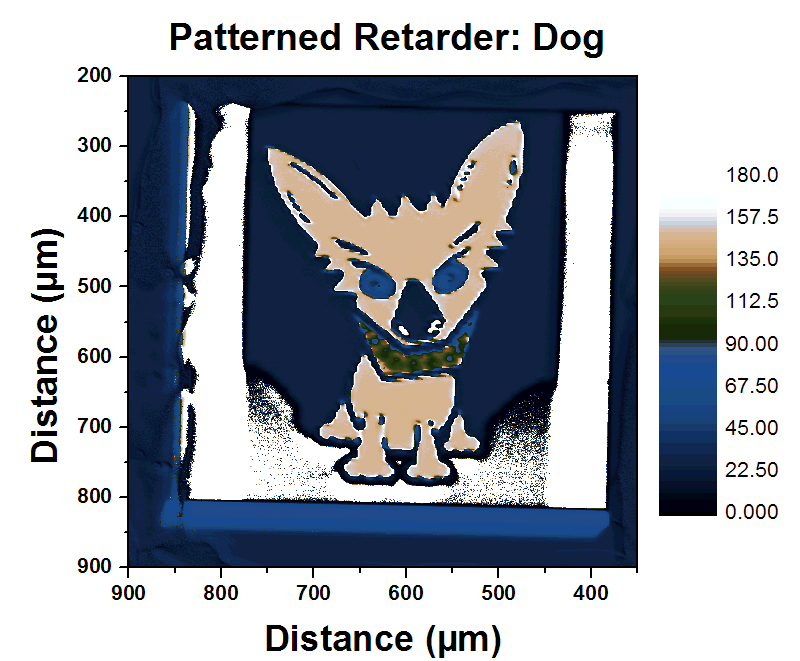
Click to Enlarge
Figure 97C Patterned Retarder with a Pictoral Distribution
| Table 8.1 Damage Threshold Specifications | ||
|---|---|---|
| Item # Suffix | Laser Type | Damage Threshold |
| -532 to 633 |
CW | 5 W/cm (810 nm, Ø0.004 mm)a |
| Pulsed (ns) | 1.8 J/cm2 (532 nm, 8 ns, 10 Hz, Ø0.200 mm) | |
| Pulsed (fs) | 0.041 J/cm2 (532 nm, 100 Hz, 76 fs, Ø162 µm) | |
| -705 to 980 | CW | 5 W/cm (810 nm, Ø0.004 mm)a |
| Pulsed (ns) | 8 J/cm2 (810 nm, 10 ns, 10 Hz, Ø0.08 mm) | |
| Pulsed (fs) | 0.041 J/cm2 (800 nm, 100 Hz, 36.4 fs, Ø189 µm) | |
| -1064 to 1550 | CW | 5 W/cm (1542 nm, Ø0.161 mm) |
| Pulsed (ns) | 10 J/cm2 (1550 nm, 7.8 ns, 10 Hz, Ø0.191 mm) | |
| Pulsed (fs) | 0.11 J/cm2 (1550 nm, 100 Hz, 70 fs, Ø145 µm) | |
Damage Threshold Data for Thorlabs' LCP Vortex Retarders
The specifications in Table 8.1 are measured data for Thorlabs' LCP vortex retarders. Damage threshold specifications are constant for all of the vortex retarders with the same AR coating.
Laser Induced Damage Threshold Tutorial
The following is a general overview of how laser induced damage thresholds are measured and how the values may be utilized in determining the appropriateness of an optic for a given application. When choosing optics, it is important to understand the Laser Induced Damage Threshold (LIDT) of the optics being used. The LIDT for an optic greatly depends on the type of laser you are using. Continuous wave (CW) lasers typically cause damage from thermal effects (absorption either in the coating or in the substrate). Pulsed lasers, on the other hand, often strip electrons from the lattice structure of an optic before causing thermal damage. Note that the guideline presented here assumes room temperature operation and optics in new condition (i.e., within scratch-dig spec, surface free of contamination, etc.). Because dust or other particles on the surface of an optic can cause damage at lower thresholds, we recommend keeping surfaces clean and free of debris. For more information on cleaning optics, please see our Optics Cleaning tutorial.
Testing Method
Thorlabs' LIDT testing is done in compliance with ISO/DIS 11254 and ISO 21254 specifications.
First, a low-power/energy beam is directed to the optic under test. The optic is exposed in 10 locations to this laser beam for 30 seconds (CW) or for a number of pulses (pulse repetition frequency specified). After exposure, the optic is examined by a microscope (~100X magnification) for any visible damage. The number of locations that are damaged at a particular power/energy level is recorded. Next, the power/energy is either increased or decreased and the optic is exposed at 10 new locations. This process is repeated until damage is observed. The damage threshold is then assigned to be the highest power/energy that the optic can withstand without causing damage. A histogram such as that shown in Figure 37B represents the testing of one BB1-E02 mirror.
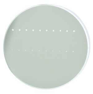
Figure 37A This photograph shows a protected aluminum-coated mirror after LIDT testing. In this particular test, it handled 0.43 J/cm2 (1064 nm, 10 ns pulse, 10 Hz, Ø1.000 mm) before damage.
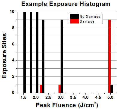
Figure 37B Example Exposure Histogram used to Determine the LIDT of
| Table 37C Example Test Data | |||
|---|---|---|---|
| Fluence | # of Tested Locations | Locations with Damage | Locations Without Damage |
| 1.50 J/cm2 | 10 | 0 | 10 |
| 1.75 J/cm2 | 10 | 0 | 10 |
| 2.00 J/cm2 | 10 | 0 | 10 |
| 2.25 J/cm2 | 10 | 1 | 9 |
| 3.00 J/cm2 | 10 | 1 | 9 |
| 5.00 J/cm2 | 10 | 9 | 1 |
According to the test, the damage threshold of the mirror was 2.00 J/cm2 (532 nm, 10 ns pulse, 10 Hz, Ø0.803 mm). Please keep in mind that these tests are performed on clean optics, as dirt and contamination can significantly lower the damage threshold of a component. While the test results are only representative of one coating run, Thorlabs specifies damage threshold values that account for coating variances.
Continuous Wave and Long-Pulse Lasers
When an optic is damaged by a continuous wave (CW) laser, it is usually due to the melting of the surface as a result of absorbing the laser's energy or damage to the optical coating (antireflection) [1]. Pulsed lasers with pulse lengths longer than 1 µs can be treated as CW lasers for LIDT discussions.
When pulse lengths are between 1 ns and 1 µs, laser-induced damage can occur either because of absorption or a dielectric breakdown (therefore, a user must check both CW and pulsed LIDT). Absorption is either due to an intrinsic property of the optic or due to surface irregularities; thus LIDT values are only valid for optics meeting or exceeding the surface quality specifications given by a manufacturer. While many optics can handle high power CW lasers, cemented (e.g., achromatic doublets) or highly absorptive (e.g., ND filters) optics tend to have lower CW damage thresholds. These lower thresholds are due to absorption or scattering in the cement or metal coating.
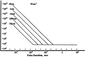
Figure 37D LIDT in linear power density vs. pulse length and spot size. For long pulses to CW, linear power density becomes a constant with spot size. This graph was obtained from [1].
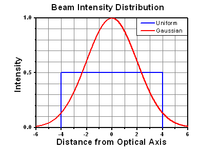
Figure 37E Intensity Distribution of Uniform and Gaussian Beam Profiles
Pulsed lasers with high pulse repetition frequencies (PRF) may behave similarly to CW beams. Unfortunately, this is highly dependent on factors such as absorption and thermal diffusivity, so there is no reliable method for determining when a high PRF laser will damage an optic due to thermal effects. For beams with a high PRF both the average and peak powers must be compared to the equivalent CW power. Additionally, for highly transparent materials, there is little to no drop in the LIDT with increasing PRF.
In order to use the specified CW damage threshold of an optic, it is necessary to know the following:
- Wavelength of your laser
- Beam diameter of your beam (1/e2)
- Approximate intensity profile of your beam (e.g., Gaussian)
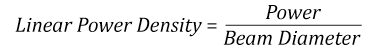
- Linear power density of your beam (total power divided by 1/e2 beam diameter)
Thorlabs expresses LIDT for CW lasers as a linear power density measured in W/cm. In this regime, the LIDT given as a linear power density can be applied to any beam diameter; one does not need to compute an adjusted LIDT to adjust for changes in spot size, as demonstrated in Figure 37D. Average linear power density can be calculated using this equation.
This calculation assumes a uniform beam intensity profile. You must now consider hotspots in the beam or other non-uniform intensity profiles and roughly calculate a maximum power density. For reference, a Gaussian beam typically has a maximum power density that is twice that of the uniform beam (see Figure 37E).
Now compare the maximum power density to that which is specified as the LIDT for the optic. If the optic was tested at a wavelength other than your operating wavelength, the damage threshold must be scaled appropriately. A good rule of thumb is that the damage threshold has a linear relationship with wavelength such that as you move to shorter wavelengths, the damage threshold decreases (i.e., a LIDT of 10 W/cm at 1310 nm scales to 5 W/cm at 655 nm):
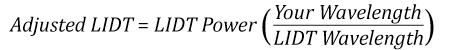
While this rule of thumb provides a general trend, it is not a quantitative analysis of LIDT vs wavelength. In CW applications, for instance, damage scales more strongly with absorption in the coating and substrate, which does not necessarily scale well with wavelength. While the above procedure provides a good rule of thumb for LIDT values, please contact Tech Support if your wavelength is different from the specified LIDT wavelength. If your power density is less than the adjusted LIDT of the optic, then the optic should work for your application.
Please note that we have a buffer built in between the specified damage thresholds online and the tests which we have done, which accommodates variation between batches. Upon request, we can provide individual test information and a testing certificate. The damage analysis will be carried out on a similar optic (customer's optic will not be damaged). Testing may result in additional costs or lead times. Contact Tech Support for more information.
Pulsed Lasers
As previously stated, pulsed lasers typically induce a different type of damage to the optic than CW lasers. Pulsed lasers often do not heat the optic enough to damage it; instead, pulsed lasers produce strong electric fields capable of inducing dielectric breakdown in the material. Unfortunately, it can be very difficult to compare the LIDT specification of an optic to your laser. There are multiple regimes in which a pulsed laser can damage an optic and this is based on the laser's pulse length. The highlighted columns in Table 37F outline the relevant pulse lengths for our specified LIDT values.
Pulses shorter than 10-9 s cannot be compared to our specified LIDT values with much reliability. In this ultra-short-pulse regime various mechanics, such as multiphoton-avalanche ionization, take over as the predominate damage mechanism [2]. In contrast, pulses between 10-7 s and 10-4 s may cause damage to an optic either because of dielectric breakdown or thermal effects. This means that both CW and pulsed damage thresholds must be compared to the laser beam to determine whether the optic is suitable for your application.
| Table 37F Laser Induced Damage Regimes | ||||
|---|---|---|---|---|
| Pulse Duration | t < 10-9 s | 10-9 < t < 10-7 s | 10-7 < t < 10-4 s | t > 10-4 s |
| Damage Mechanism | Avalanche Ionization | Dielectric Breakdown | Dielectric Breakdown or Thermal | Thermal |
| Relevant Damage Specification | No Comparison (See Above) | Pulsed | Pulsed and CW | CW |
When comparing an LIDT specified for a pulsed laser to your laser, it is essential to know the following:
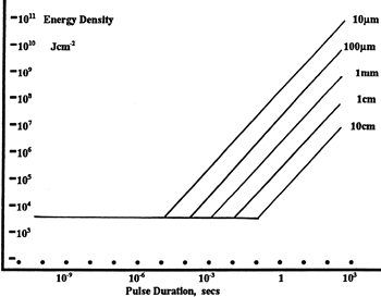
Figure 37G LIDT in energy density vs. pulse length and spot size. For short pulses, energy density becomes a constant with spot size. This graph was obtained from [1].
- Wavelength of your laser
- Energy density of your beam (total energy divided by 1/e2 area)
- Pulse length of your laser
- Pulse repetition frequency (prf) of your laser
- Beam diameter of your laser (1/e2 )
- Approximate intensity profile of your beam (e.g., Gaussian)
The energy density of your beam should be calculated in terms of J/cm2. Figure 37G shows why expressing the LIDT as an energy density provides the best metric for short pulse sources. In this regime, the LIDT given as an energy density can be applied to any beam diameter; one does not need to compute an adjusted LIDT to adjust for changes in spot size. This calculation assumes a uniform beam intensity profile. You must now adjust this energy density to account for hotspots or other nonuniform intensity profiles and roughly calculate a maximum energy density. For reference a Gaussian beam typically has a maximum energy density that is twice that of the 1/e2 beam.
Now compare the maximum energy density to that which is specified as the LIDT for the optic. If the optic was tested at a wavelength other than your operating wavelength, the damage threshold must be scaled appropriately [3]. A good rule of thumb is that the damage threshold has an inverse square root relationship with wavelength such that as you move to shorter wavelengths, the damage threshold decreases (i.e., a LIDT of 1 J/cm2 at 1064 nm scales to 0.7 J/cm2 at 532 nm):
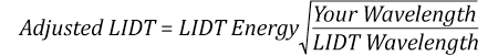
You now have a wavelength-adjusted energy density, which you will use in the following step.
Beam diameter is also important to know when comparing damage thresholds. While the LIDT, when expressed in units of J/cm², scales independently of spot size; large beam sizes are more likely to illuminate a larger number of defects which can lead to greater variances in the LIDT [4]. For data presented here, a <1 mm beam size was used to measure the LIDT. For beams sizes greater than 5 mm, the LIDT (J/cm2) will not scale independently of beam diameter due to the larger size beam exposing more defects.
The pulse length must now be compensated for. The longer the pulse duration, the more energy the optic can handle. For pulse widths between 1 - 100 ns, an approximation is as follows:
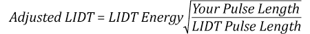
Use this formula to calculate the Adjusted LIDT for an optic based on your pulse length. If your maximum energy density is less than this adjusted LIDT maximum energy density, then the optic should be suitable for your application. Keep in mind that this calculation is only used for pulses between 10-9 s and 10-7 s. For pulses between 10-7 s and 10-4 s, the CW LIDT must also be checked before deeming the optic appropriate for your application.
Please note that we have a buffer built in between the specified damage thresholds online and the tests which we have done, which accommodates variation between batches. Upon request, we can provide individual test information and a testing certificate. Contact Tech Support for more information.
[1] R. M. Wood, Optics and Laser Tech. 29, 517 (1998).
[2] Roger M. Wood, Laser-Induced Damage of Optical Materials (Institute of Physics Publishing, Philadelphia, PA, 2003).
[3] C. W. Carr et al., Phys. Rev. Lett. 91, 127402 (2003).
[4] N. Bloembergen, Appl. Opt. 12, 661 (1973).

In order to illustrate the process of determining whether a given laser system will damage an optic, a number of example calculations of laser induced damage threshold are given below. For assistance with performing similar calculations, we provide a spreadsheet calculator that can be downloaded by clicking the LIDT Calculator button. To use the calculator, enter the specified LIDT value of the optic under consideration and the relevant parameters of your laser system in the green boxes. The spreadsheet will then calculate a linear power density for CW and pulsed systems, as well as an energy density value for pulsed systems. These values are used to calculate adjusted, scaled LIDT values for the optics based on accepted scaling laws. This calculator assumes a Gaussian beam profile, so a correction factor must be introduced for other beam shapes (uniform, etc.). The LIDT scaling laws are determined from empirical relationships; their accuracy is not guaranteed. Remember that absorption by optics or coatings can significantly reduce LIDT in some spectral regions. These LIDT values are not valid for ultrashort pulses less than one nanosecond in duration.
Figure 71A A Gaussian beam profile has about twice the maximum intensity of a uniform beam profile.
CW Laser Example
Suppose that a CW laser system at 1319 nm produces a 0.5 W Gaussian beam that has a 1/e2 diameter of 10 mm. A naive calculation of the average linear power density of this beam would yield a value of 0.5 W/cm, given by the total power divided by the beam diameter:
However, the maximum power density of a Gaussian beam is about twice the maximum power density of a uniform beam, as shown in Figure 71A. Therefore, a more accurate determination of the maximum linear power density of the system is 1 W/cm.
An AC127-030-C achromatic doublet lens has a specified CW LIDT of 350 W/cm, as tested at 1550 nm. CW damage threshold values typically scale directly with the wavelength of the laser source, so this yields an adjusted LIDT value:
The adjusted LIDT value of 350 W/cm x (1319 nm / 1550 nm) = 298 W/cm is significantly higher than the calculated maximum linear power density of the laser system, so it would be safe to use this doublet lens for this application.
Pulsed Nanosecond Laser Example: Scaling for Different Pulse Durations
Suppose that a pulsed Nd:YAG laser system is frequency tripled to produce a 10 Hz output, consisting of 2 ns output pulses at 355 nm, each with 1 J of energy, in a Gaussian beam with a 1.9 cm beam diameter (1/e2). The average energy density of each pulse is found by dividing the pulse energy by the beam area:
As described above, the maximum energy density of a Gaussian beam is about twice the average energy density. So, the maximum energy density of this beam is ~0.7 J/cm2.
The energy density of the beam can be compared to the LIDT values of 1 J/cm2 and 3.5 J/cm2 for a BB1-E01 broadband dielectric mirror and an NB1-K08 Nd:YAG laser line mirror, respectively. Both of these LIDT values, while measured at 355 nm, were determined with a 10 ns pulsed laser at 10 Hz. Therefore, an adjustment must be applied for the shorter pulse duration of the system under consideration. As described on the previous tab, LIDT values in the nanosecond pulse regime scale with the square root of the laser pulse duration:
This adjustment factor results in LIDT values of 0.45 J/cm2 for the BB1-E01 broadband mirror and 1.6 J/cm2 for the Nd:YAG laser line mirror, which are to be compared with the 0.7 J/cm2 maximum energy density of the beam. While the broadband mirror would likely be damaged by the laser, the more specialized laser line mirror is appropriate for use with this system.
Pulsed Nanosecond Laser Example: Scaling for Different Wavelengths
Suppose that a pulsed laser system emits 10 ns pulses at 2.5 Hz, each with 100 mJ of energy at 1064 nm in a 16 mm diameter beam (1/e2) that must be attenuated with a neutral density filter. For a Gaussian output, these specifications result in a maximum energy density of 0.1 J/cm2. The damage threshold of an NDUV10A Ø25 mm, OD 1.0, reflective neutral density filter is 0.05 J/cm2 for 10 ns pulses at 355 nm, while the damage threshold of the similar NE10A absorptive filter is 10 J/cm2 for 10 ns pulses at 532 nm. As described on the previous tab, the LIDT value of an optic scales with the square root of the wavelength in the nanosecond pulse regime:
This scaling gives adjusted LIDT values of 0.08 J/cm2 for the reflective filter and 14 J/cm2 for the absorptive filter. In this case, the absorptive filter is the best choice in order to avoid optical damage.
Pulsed Microsecond Laser Example
Consider a laser system that produces 1 µs pulses, each containing 150 µJ of energy at a repetition rate of 50 kHz, resulting in a relatively high duty cycle of 5%. This system falls somewhere between the regimes of CW and pulsed laser induced damage, and could potentially damage an optic by mechanisms associated with either regime. As a result, both CW and pulsed LIDT values must be compared to the properties of the laser system to ensure safe operation.
If this relatively long-pulse laser emits a Gaussian 12.7 mm diameter beam (1/e2) at 980 nm, then the resulting output has a linear power density of 5.9 W/cm and an energy density of 1.2 x 10⁻⁴ J/cm2 per pulse. This can be compared to the LIDT values for a WPQ10E-980 polymer zero-order quarter-wave plate, which are 5 W/cm for CW radiation at 810 nm and 5 J/cm2 for a 10 ns pulse at 810 nm. As before, the CW LIDT of the optic scales linearly with the laser wavelength, resulting in an adjusted CW value of 6 W/cm at 980 nm. On the other hand, the pulsed LIDT scales with the square root of the laser wavelength and the square root of the pulse duration, resulting in an adjusted value of 55 J/cm2 for a 1 µs pulse at 980 nm. The pulsed LIDT of the optic is significantly greater than the energy density of the laser pulse, so individual pulses will not damage the wave plate. However, the large average linear power density of the laser system may cause thermal damage to the optic, much like a high-power CW beam.
| Posted Comments: | |
Nohyoon Park
(posted 2025-10-19 22:19:30.22) Hello,
I am using a broadband continuum light source spanning 500–600 nm, and I’m looking for a vortex half-wave plate (VHWP) suitable for this range.
Could you please let me know:
1. Whether you can custom-fabricate a VHWP that maintains half-wave retardance across 500–600 nm, and
2. If not, which existing model (e.g., WPV10L-532, WPV10L-633, etc.) would be most appropriate for this spectral range?
Thank you jdelia
(posted 2025-10-22 07:47:16.0) Thank you for contacting Thorlabs. Our achromatic vortex retarders are currently under development, and we will reach out to you directly to discuss the possibility of offering this. For future custom requests, please feel free to contact your local technical support team (in your case: techsales@thorlabs.com). sandi kumar
(posted 2025-08-12 22:23:55.897) Dear Thorlabs team, I am a little bit confused by the description given in the comparison tab. There it is stated that the vortex half wave retarder with m=1 generates a vortex pattern with m=2. Are you referring there to an LG-mode with topological charge 2? According to the equation and m=1, this would refer to a q-plate with q=1/2, which, if I am not mistaken, leads to a beam of charge equals to m = 2*q = 2 * 1/2 = 1. Now I am a bit confused as your description says, that a m=1 order generates a m=2 vortex pattern. So in the case I am using a lin. polarized Gaussian beam together with a m=1 vortex half-wave retarder, do I get a m=2 vortex beam? Thank you in advance! jdelia
(posted 2025-08-15 08:01:42.0) Thank you for contacting Thorlabs! In our definition, m indicates that the polarization rotates by 180 degrees as it goes around a complete cycle of the azimuth. Therefore, an m = 1 vortex half-wave retarder creates an m = 2 vortex beam, an m = 2 vortex half-wave retarder creates an m = 4 vortex beam. For a clearer visualization of the resulting beam modes, please kindly refer to the last column of Figure 4.4 in the “Comparison” tab. Jingni Geng
(posted 2025-07-10 12:14:25.98) I am currently working on calculating the practical phase retardance for my setup, but in my case, I need to use a q-plate under a wavelength that significantly deviates from the design wavelength. (I am currently using several q-plates from your WPV10 series, specifically:
WPV10L-532, WPV10L-633, WPV10L-705, WPV10L-780, WPV10L-830, and WPV10-780. However, all incident beams are at 1064 nm.)
I would like to estimate the actual phase retardance δ for each q-plate at 1064 nm. To do so, I need to confirm:
Are all of these q-plates fabricated using the same liquid crystal material?
If so, could you please provide the birefringence dispersion (i.e., Δ𝑛(𝜆) or refractive index data for the material?
If different materials are used across different models, could you kindly specify which material corresponds to each plate?
Any available information on the material properties or thickness of the liquid crystal layer would also be very helpful for accurate modeling.
Thank you in advance for your support. YLohia
(posted 2025-07-14 01:22:17.0) Thank you for contacting Thorlabs! We use the same liquid crystal material for all of our Vortex Half-Wave Retarders (as of the time of this post). The Δ𝑛 value is 0.1555 @ 550 nm. Please refer to the retardance data for our liquid crystal half-wave plates here: https://www.thorlabs.com/newgrouppage9.cfm?objectgroup_id=7054 .
The relevant data are as follows:
WPH10E-532: 0.2369 waves @ 1064 nm;
WPH10E-633: 0.2829 waves @ 1064 nm;
WPH10E-780: 0.3503 waves @ 1064 nm;
WPH10E-830: 0.3771 waves @ 1064 nm.
Unfortunately, we currently do not offer half-wave plates for 705 nm, so we are unable to provide the retardance data for WPV10L-705. We apologize for the inconvenience. Alex P
(posted 2025-06-26 06:16:17.393) Hello,
I would like to use Zero-Order Vortex Half-Wave Retarders for 808 nm. Can you tell which one is the best choice and how well it will perform?
Thank you jdelia
(posted 2025-06-27 08:05:46.0) Thank you for contacting Thorlabs. In our Zero-Order Vortex Half-Wave Retarder categories, the designed wavelength which is closest to 808 nm is 830 nm. If using WPV10L-830 or WPV10-830 with an 808 nm laser, the retardance changes to 0.514λ, which is a 2.7% error with respect to the half wave. The quality of the generated vortex beam will be affected. We have customization capability to offer vortex retarders with a center wavelength of 808 nm. For future customization inquiries, please feel free to reach out to your local technical sales team (in your case: techsales@thorlabs.com). Ivor Leung
(posted 2025-06-09 17:44:55.09) Hi,
I am looking for a vortex phase plate with center wavelength 785nm and topological charge m = 1 (similar to WPV10L-780). Can you give me a quote (price and lead time) for this request? Thank you. jdelia
(posted 2025-06-11 04:48:52.0) Thank you for contacting Thorlabs. We can provide a vortex phase plate with center wavelength 785nm and topological charge m = 1. We will contact you directly to offer you with a quote. For future customization inquiries, please feel free to reach out to your local technical sales team (in your case: techsales@thorlabs.com). Liat L
(posted 2025-06-09 17:06:42.207) Hello!
I am looking for a q-plate that for a right circularly polarized (RCP) Gaussian beam, the output beam is left circularly polarized (LCP) Laguerre-Gaussian beam with topological charge l = -1 and for LCP light the output beam is RCP with l=1 (the opposite).
Meaning, that it flips the polarization and adds or substructs one quanta of OAM. Does these Vortex Half-Wave Retarders can do such a mechanism? I am not sure from looking into them on your site. Specifically, I am interested in the product WPV10L-830.
Thanks in advance for your answer! Liat jdelia
(posted 2025-06-10 08:04:41.0) Thank you for contacting Thorlabs. In theory, a WPV is a half-wave plate with a specific azimuth pattern, so it should change the handedness of the input beam to the orthogonal one. Regarding the output mode, Lorenzo Marrucci's paper (cf. J Opt 13, 064001 (2011) Fig. 2) referred to the output beam mode as helical mode. user
(posted 2025-02-26 14:26:24.857) We are looking into shaping of a 637nm laser beam and were wondering for the 4pi phase plate with design wavelength 633nm (WPV10-633) how well the 0 intensity in the center is maintained by the wavelength mismatch cdolbashian
(posted 2025-03-19 12:35:31.0) Thank you for contacting Thorlabs. Our experience is that if there is a large wavelength mismatch, then the center of the beam does not reach zero intensity. That being said, 637 nm is very close to 633 nm, and we would expect the 4nm offset to be negligible. Therefore, you may use the 633 nm version. Jordi Tiana Alsina
(posted 2024-10-04 17:38:34.433) Dear Technical Department,
I am generating doughnut beam profiles for super-resolution microscopy applications and would like to inquire if you have a vortex retarder tuned to 488 nm.
Thank you in advance for your assistance.
Best regards,
Jordi fmortaheb
(posted 2024-10-08 11:08:13.0) Thank you for contacting Thorlabs. We can offer a custom 488 nm vortex waveplate. We will reach out to you directly to discuss offering this special item. Dmitry Kovba
(posted 2024-09-07 12:56:42.22) Hi! What’s the highest order (m) of a vortex half-wave retarder can you manufacture? Can you make it 2” in diameter? cdolbashian
(posted 2024-09-17 03:45:41.0) Thank you for contacting Thorlabs. The highest order (m) of a vortex half-wave retarder we can manufacture is, in principle, m=640. However, as the order m increases, we expect the center singularity point to also increase. In reference to the maximum size, currently, we are able to manufacture a 1" diameter. For future custom requests, please feel free to reach out to your local tech support team (in your case: techsupport@thorlabs.com). Matthias Kübel
(posted 2024-07-01 07:13:47.9) The CW damage threshold for the vortex retarders is specified in units of W/cm. Presumably, these are supposed to be W/cm^2 ?
Best regards
Matthias cdolbashian
(posted 2024-07-12 02:35:12.0) Thank you for contacting Thorlabs. We express laser induced damage threshold for CW lasers as a linear power density measured in W/cm. In this regime, the damage threshold given as a linear power density can be applied to any beam diameter. For more details about the damage threshold, please refer to the "Damage Thresholds" tab (link: https://www.thorlabs.com/newgrouppage9.cfm?objectgroup_id=9098&tabname=Damage_Thresholds). user
(posted 2024-06-24 10:25:26.93) What is the difference between the angels of the m=1-plate in fig.3 in the comparison tab. So, by how many degrees was the plate rotated to obtain azimuthal polarisation instead of radial polarisation with the same input polarisation? cdolbashian
(posted 2024-06-28 11:58:57.0) Thank you for contacting Thorlabs. For m = 1 vortex half-wave plates, the 3 lines on the housing indicate the zero-degree fast axis. When the 3 lines are parallel to the input polarization, the output is a radial polarization beam. Rotating the wave plates in any direction for 90 degrees, the output will turn to an azimuthal polarization beam. user
(posted 2023-11-19 14:28:35.67) Dear Thorlabs team,
I am a little bit confused by the description given in the comparison tab. There it is stated that the vortex half wave retarder with m=1 generates a vortex pattern with m=2. Are you referring there to an LG-mode with topological charge 2?
According to the equation and m=1, this would refer to a q-plate with q=1/2, which, if I am not mistaken, leads to a beam of charge equals to m = 2*q = 2 * 1/2 = 1. Now I am a bit confused as your description says, that a m=1 order generates a m=2 vortex pattern.
So in the case I am using a lin. polarized Gaussian beam together with a m=1 vortex half-wave retarder, do I get a m=2 vortex beam?
Thank you in advance! Tom Brain
(posted 2023-10-23 09:47:34.857) Hi, I'd like to post a correction to the information contained in the product overview. It states: "Vortex retarders generate nondiffracting, or Bessel, beams". While Bessel functions can be made to produce this intensity distribution using specific parameters, it's an awkward label, and is much better described by Laguerre-Gaussian functions. It would possibly be best to edit this to avoid uncertainty for customers. cdolbashian
(posted 2023-11-08 12:17:19.0) Thank you for reaching out to us with this helpful insight! We will update the expression on the website accordingly. Valeriia Ahlborn
(posted 2022-08-16 14:53:16.263) Hello,
is it correct, that when going to a q-plate with a right circularly polarized (RCP) Gaussian beam, the outgoing beam is left circularly polarized (LCP) Laguerre-Gaussian beam with topological charge l = -1 and the opposite sign of topological charge l = 1, when the incoming beam is LCP? in other words if the LG beam is LCP after the q-plate it's topological charge is defined as l = -1. Does it depend on the orientation of the q-plate?
Thanks in advance for your answer.
Sincerely yours,
Valeriia Ahlborn cdolbashian
(posted 2022-09-07 02:57:22.0) Thank you for contacting Thorlabs. In principle, a WPV is a half-wave plate but with a specific azimuth pattern. It should turn a left circularly polarized input beam into a right circularly polarized beam, and vice-versa. They are independent of the orientation of the vortex half-wave plate. For the relationship between LCP/RCP and their corresponding output states, one can refer to the description in Lorenzo Marrucci's paper (cf. J Opt 13, 064001 (2011) Fig. 2). jeongsoo kim
(posted 2022-05-26 23:51:37.547) May I know the retardation information of the product(WPV10L-532)? cdolbashian
(posted 2022-05-27 12:21:37.0) Thank you for reaching out to us with this inquiry. The retardation for this product is λ/2 at 532nm. This information can be found under the "Specs" tab above. user
(posted 2021-11-15 02:13:38.073) I am curious about the name that has been given for this product like "zero-order vortex " even for m=1 or m=2. What does this order signify for this name? Can you please explain this? YLohia
(posted 2021-11-23 02:04:35.0) Thank you for contacting Thorlabs. The retardance produced by a half-wave plate is (n+1/2)*wavelength. "Zero-order" refers to n=0. The difference between the two m orders is the fast axis distribution over the clear aperture of the retarder, where m is the order in the equation shown under "Comparison" tab. Mostafa Youssef
(posted 2021-09-17 11:23:52.643) I want to know if this plate convert a gaussian beam to OAM +\- 1 and radial and azimuthal beams? YLohia
(posted 2021-09-20 10:19:32.0) Thank you for contacting Thorlabs. Yes, the WPV10L-1550 can convert a gaussian beam to OAM +/-1 beams. For radial and azimuthal polarization information, please refer to the information listed in the "Comparison" tab. user
(posted 2021-08-06 09:43:20.057) Do your vortex plates behave like the q-plates described by Delaney (DELANEY, Sam, SÁNCHEZ-LÓPEZ, María M., MORENO, Ignacio, et al. Arithmetic with q-plates. Applied optics, 2017, vol. 56, no 3, p. 596-600)? Is Delaney's equation 1 valid for your vortex plates? Is it possible to add/substract your vortex plates the way it is shown at Delaney's section 3.2-3.3? Thank you for the help. YLohia
(posted 2021-08-27 02:03:12.0) Thank you for contacting Thorlabs. "The q-plate consists of a linear phase plate retarder with a retardance of π radians where the principal axis of the retarder follows q times the azimuthal angle θ" The description of q-plates in Delaney's paper is correct for describing our vortex plates. Theoretically, the equations you mentioned should be applicable. David M
(posted 2021-06-28 07:12:34.853) Hi. I am curious to know how is the central part of the beam after the vortex retarder, when it is illuminated with a linearly polarized Gaussian beam. I mean, how is the polarization and the intensity of the ligh at the center? Thanks. YLohia
(posted 2021-07-01 10:30:35.0) Hello, the central part of the beam can be referred to as a "singularity point". Our vortex retarders create a donut hole beam profile from a Gaussian beam. It is a ring beam with zero intensity at the center. There is no light in the center (and, therefore, no polarization state on the output due to the absence of light). Kadgu Ragha
(posted 2021-05-31 16:10:22.49) Hi,
I am curious to know what exactly is the fast-axis orientation of the fabricated vortex wave retarder, at its origin i.e, at x=0 and y=0.? Apparently, the fast-axis at this point is not well defined mathematically, what do you do..? YLohia
(posted 2021-06-04 02:48:48.0) Thank you for contacting Thorlabs. The very center of a vortex wave retarder is what can be referred to as a "singularity point", which means that the fast-axis is undefined. In practice, there is a small area (<30 um) of random fast-axis distribution due to the manufacturing process. Such a random pattern is unique to each piece. Alexey Petrov
(posted 2021-05-24 23:10:40.877) Good afternoon, please tell me what is the damage threshold for WPV10-780 and WPV10-780? Parameters of our setup: Pulse duration 60 fs, wavelength 800nm, pulse repetition rate 10 Hz, beam radius 1,25cm. Gaussian profile.
thank you! YLohia
(posted 2021-05-27 02:36:46.0) Hello, thank you for contacting Thorlabs. Please refer to the information under "Damage Thresholds" tab: -705 to 980 nm, 0.041 J/cm2 (800 nm, 100 Hz, 36.4 fs, Ø189 µm). Since the LIDT for fs pulsed laser is not scalable, we would recommend starting with the lowest possible input power and then ramping up slowly. Markus Stabel
(posted 2021-04-30 10:02:29.34) Do you have any data on the polarization distribution when using your Vortex plates with a circular polarized beam?
According to some comments here and my research, the vortex plates seem to be equivalent to so-called q-plates with q=m/2. Then according to Filippo Cardano, Ebrahim Karimi, Sergei Slussarenko, Lorenzo Marrucci, Corrado de Lisio, and Enrico Santamato, "Polarization pattern of vector vortex beams generated by q-plates with different topological charges," Appl. Opt. 51, C1-C6 (2012) the circular polarization would be inverted in the resulting Laguerre Gaussian mode, e.g. left circular input polarization would be turned to right circular polarization and the polarization distribution would be uniform over the entire donut beam profile. Can you confirm this behavior with your Vortex plates? Thanks for the help. YLohia
(posted 2021-05-10 08:09:15.0) Thank you for contacting Thorlabs. Our vortex half-wave plate is essentially a half-wave plate with varying fast-axis distribution. In theory, it should turn a left circularly polarized input beam into a right circularly polarized beam, and vice-versa. Though due to the patterned nature of the waveplate, there is some non-uniformity in retardance, which would slightly affect the resultant polarization distribution. We have also released the fast axis pattern of these LCP vortex retarders. If interested in this, please refer to the "Comparison" tab. RK KB
(posted 2020-11-18 06:38:33.213) When vortex waveretarders are used with high energy pulsed light sources and within the suggested LIDT range, will there be any degradation in the "patterning"..? In other words, whether the suggested LIDT range accounts for the material damage or (material + property) damage..? YLohia
(posted 2020-11-19 10:48:44.0) Thank you for contacting Thorlabs. The liquid crystals and alignment materials are cured before shipment, so assuming there is no physical damage during the shipping, the "patterning" will also remain undamaged. One exception to this would be if the LC material is exposed to UV light as that would reduce the retardance (but no notable visible damage). David Guyton
(posted 2020-10-12 09:48:55.283) In the Comparison tab on your website for your vortex retarders, the fast axis distribution for your m=2 vortex retarders is exactly radial in Figure 3, but is not exactly radial in Figure 2, especially in the horizontal meridian. Which is correct? Is the drawing wrong in Fig. 2?
Thanks / David Guyton YLohia
(posted 2020-10-15 09:23:12.0) Thank you for contacting Thorlabs. Figure 2 contains experimental data measured using the LCC7201 and the WPV while Figure 3 is generated from theoretical data. The direction of the polarization direction arrows (0 deg and 180 deg) are the same. Yongguang zhao
(posted 2020-09-08 11:27:49.003) Are these vortex Relarders used for producing vector vortex beams? Could you provide some producations used for generation of scalar vortex beams. YLohia
(posted 2020-09-09 08:53:20.0) Hello, thank you for contacting Thorlabs. Our WPV series vortex retarders produce a polarization singularity, which, by definition, is a vector vortex beam. In order to produce a scalar vortex beam (phase singularity), one requires a spiral phase wavefront which can be generated by our EXULUS series spatial light modulators. The EXULUS-HD2/HD3/HD4 software contains vortex generation features. The EXULUS-HD1 and EXULUS-4K1 will also have this functionality with an upcoming software update. user
(posted 2020-05-20 14:08:11.923) I'm curious about the performance of each of these over a larger bandwidth transmission? Does the 532nm waveplate have +- some bandwidth with >90% transmission for example?
The specs and graph tabs have labels for multiple plates, so it is difficult to discern the bandwidth performance for a single plate. YLohia
(posted 2020-05-21 08:54:34.0) Thank you for contacting Thorlabs. The design wavelength for a given vortex retarder is specified for its "Retardance". For the WPV10-532, for example, only 532 nm light will undergo lambda/2 retardance. If you would like to generate a donut beam, a few tens of nm bandwidth would be fine, though the phase won't be half wave. As for the transmission, since the WPV10-532 uses the same substrate and coating as the 405 nm and 633 nm vortex plates, you may just refer to the transmission vs wavelength figure under "Graphs" on the page. >90% transmission covers the wavelength range from 405 nm to 700 nm. Sebastien Loranger
(posted 2020-04-01 10:18:29.367) Just a suggestion:
The vortex retarders can convert OAM states (LG beams) when the input polarisation is circular. These are essentially q-plates (q=m/2) as described in
M. Lorenzo, K. Ebrahim, S. Sergei, P. Bruno, S. Enrico, N. Eleonora, and S. Fabio, "Spin-to-orbital conversion of the angular momentum of light and its classical and quantum applications," Journal of Optics 13, 064001 (2011).
I could be worth mentioning... (currently only the effect of linear polarisation is mentioned in the information) YLohia
(posted 2020-04-03 11:58:49.0) Thank you for your feedback and suggestions. Our wave plate retarders are based on varying fast-axis distributions. We emphasize that to avoid confusion and also because there are also other configurations on the market (for example, helical phase distribution). We have demonstrated linearly polarized inputs as one of the many ideas, and it is true that potential applications are certainly not limited to just that. Conversion of OAM states is also another major application of q-plates. user
(posted 2020-02-18 07:20:10.453) Hello,
For a retarder build to work at 532 nm, what would be the polarization conversion efficiency at 527 nm ? Do you have this kind of specs ?
Thank you nbayconich
(posted 2020-02-19 11:20:53.0) Thank you contacting Thorlabs. You may scale the retardance of WPV10-532 at 527nm to be: (527/532)*λ/2. If you only would like a donut beam, you may try WPV10-532 at 527nm. If your application requires to have an exact lambda/2 retardance at 527nm, a customized WPV10 at your working wavelength is suggested. lindenjhn
(posted 2019-01-02 06:38:05.533) Hi, do you have a quality measurement of the percent output polarization as desired from the beam? compared also to an optimal polarization?
Also would you have an element for 350nm range?
Thanks. nbayconich
(posted 2019-01-10 08:49:41.0) Thank you for contacting Thorlabs. Would it be possible to clarify what you mean by quality measurement regarding the percent output polarization as desired? In terms of quality we do not specify the fast axis alignment tolerance. As stated these vortex retarders will create a spatially varying polarization state and phase output of your input source.
I will reach out to you directly to discuss our custom capabilities. c.kelly.4
(posted 2018-12-10 12:05:49.197) Hello, I would like to ask if these vortex retarders introduce a spatially varying phase to the gaussian input beam, such that a helical wavefront is produced giving a light beam with orbital angular momentum? Is this in addition to a spatially varying polarisation? Thank you very much for your help. nbayconich
(posted 2019-01-03 10:37:24.0) Thank you for contacting Thorlabs, yes that is correct the vortex wave retarders have a spatially varying fast axis which produces a spatially varying phase in your sources's wavefront. In doing so this introduces orbital angular momentum as a result of creating a helical wavefront, these helical modes are determined by the m order number. This also induces a spatially varying polarization state of your source as a result of the spatially varying fast axis distribution across the vortex retarder.
Under the comparison tab on our Vortex half wave retarders page several pictures of the fast axis distribution of both the m = 1 & m =2 vortex retarders can be seen as well as the resultant output polarization with respect to a linearly polarized input source. thlu
(posted 2017-06-09 10:41:29.57) Hi, I am wondering what is the ne and no of this product(WPV10L-532) related to 1064 nm wavelength? I'm looking forward to the reply. Thank you so much. nbayconich
(posted 2017-07-05 09:12:39.0) Thank you for contacting Thorlabs. We do not measure the absolute index in the ordinary and extraordinary axis. For WPV10L-532 The fast axis distribution is the same at 1064nm and the corresponding retardance becomes 0.2369. I will reach out to you directly. gene.serabyn
(posted 2017-04-03 18:29:08.8) I have a question about these vortices, but couldn't find an email address to send it to, so I'll try this route. How good are the centers of these vortices? I.e., do they follow the desired vortex pattern down to, e.g., the central 1 mm, or 100 microns, or 10 microns?
Thanks,
Gene Serabyn tfrisch
(posted 2017-04-19 02:52:52.0) Hello, thank you for contacting Thorlabs. The point of rotation of the fast axis is nominally at the center of the substrate, but there will be some variation from one unit to another. The actual point will be within 1mm of the center as mentioned on the LG Mode & Alignment tab. I will reach out to you directly from TechSupport@Thorlabs.com to further discuss these vortex retarders. d.maluenda
(posted 2016-10-27 07:06:40.667) Hi, I am wondering whether Zero-Order Vortex HWP introduce an angular fase (topological charge) to the beam.
Thank you so much. tfrisch
(posted 2016-11-01 10:33:20.0) Hello, thank you for contacting Thorlabs. I have reached out to you directly about your application. prudencejade
(posted 2016-06-02 01:41:15.413) Hello,
I am wondering whether the wave plate can be used in a broadband light with bandwidth of 1400 nm.
I would like to know the variation of the retardation for such a broadband light.
I am looking forward to the reply. Thank you so much! besembeson
(posted 2016-06-02 03:15:07.0) Response from Bweh at Thorlabs USA: The tests we have done so far are with monochromatic sources. The retardation for these are wavelength dependent which will affect performance. I will contact you to further discuss your application and if we can get some test data. |

 Zoom
Zoom
Click to Enlarge
Figure G1.1 The intensity profile created by an m = 1 retarder when viewed between crossed polarizers.
- Generates an m = 2 Vortex Polarization Pattern from Linearly Polarized Light
- Center Wavelength Options from 532 nm to 1550 nm
- Large AOI of ±20°
These true zero-order, m = 1 vortex half-wave plates are designed to affect the radial and azimuthal polarization of optical fields. They have a constant retardance across the clear aperture, but a fast axis that rotates continuously over the optic (see the Graphs tab). Viewed through crossed polarizers with a while light source (see Figure G1.1), these retarders produce an intensity profile with 2 modulations. Thus, when used with a linearly polarized light source, these retarders will generate an m = 2 polarization pattern.
The donut hole intensity profile capable of being produced by the m = 1 retarder is smaller and more circular than that of the
m = 2 retarders sold below (see the Comparison tab). Additionally, these are polarization sensitive devices and will produce different output polarizations depending on the orientation of the wave plate’s fast axis to the polarization axis of the input beam.
These retarders are mounted in an aluminum housing with an engraving along the perimeter to assist in locating the center point of the plate for beam alignment purposes. The zero-degree fast axis is indicated by 3 lines.

 Zoom
Zoom
Click to Enlarge
Figure G2.1 The intensity profile created by an m = 2 retarder when viewed between crossed polarizers.
- Generates an m = 4 Vortex Polarization Pattern from Linearly Polarized Light
- Center Wavelength Options from 532 nm to 1550 nm
- Large AOI of ±20°
These true zero-order, m = 2 vortex half-wave plates are designed to affect the radial and azimuthal polarization of optical fields. They have a constant retardance across the clear aperture, but a fast axis that rotates continuously over the optic (see the Graphs tab). Viewed through crossed polarizers with a while light source (see Figure G2.1), these retarders produce an intensity profile with 4 modulations. When used with a linearly polarized light source, these retarders will generate an m = 4 polarization pattern.
The donut hole intensity profile capable of being produced by the m = 2 retarder is larger and more eliptical than that of the
m = 1 retarders sold above (see the Comparison tab).
These devices are polarization insensitive devices and will produce similar output polarizations regardless of the orientation of the wave plate’s fast axis to the polarization axis of the input beam. They are mounted in an aluminum housing with an engraving along the perimeter to assist in locating the center point of the plate for beam alignment purposes.