 Products Home / Imaging Systems / OCT Imaging Systems & Components / OCT Components / OCT Balanced Detectors / OCT Balanced Detectors with Fast Monitor Output
OCT Balanced Detectors with Fast Monitor Output
- Models Available with Bandwidths up to 2.5 GHz
- Wavelengths Covering the 320 to 1700 nm Range
- >20 dB Common Mode Rejection Ratio
- Fast Monitor Outputs
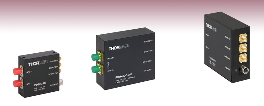
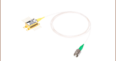
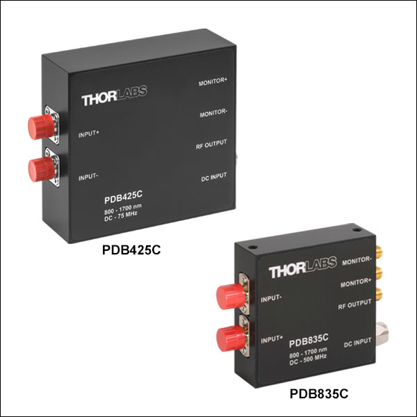
PDB835C
Fixed Gain, 500 MHz, InGaAs,
Compact, Ultra-Low Noise
Optical Inputs Shown
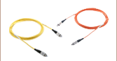
PDB482C-AC
Fixed Gain, 2.5 GHz, InGaAs, AC Coupled
Optical Inputs Shown
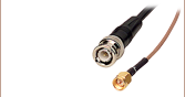
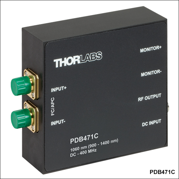
PDB440C
Fixed Gain, 15 MHz, InGaAs
Electrical Outputs Shown


Please Wait
| Balanced Detector Selection Guide |
|---|
| Balanced Detectors with Fast Monitor Output |
| Large-Area Balanced Amplified Detectors |
| Suitable for OCT |
| Compact Balanced Amplified Detectors |
| Compact Balanced Detectors |
| OCT Balanced Detectors with Fast Monitor Output |
| Auto-Balanced Detector with Avalanche Photodiodes |
| OCT Balanced Detectors with Fast Monitor Output | ||
|---|---|---|
| Wavelength | Bandwidths Available | Fast Monitor Output Bandwidth |
| 320 - 1000 nm | DC - 15 MHz DC - 75 MHz DC - 100 MHz DC - 200 MHz DC - 500 MHz |
DC - 1 MHz |
| 800 - 1700 nm | ||
| Optimized for 1060 nm (900 - 1400 nm Range) |
DC - 400 MHz 30 kHz - 1.0 GHz |
DC - 3 MHz |
| 1 MHz - 2.5 GHz | DC - 2.5 MHz | |
| Optimized for 1300 nm (1200 - 1700 nm Range) |
DC - 400 MHz 30 kHz - 1.6 GHz |
DC - 3 MHz |
Features
- Bandwidths up to 2.5 GHz Available
- Four Wavelength Options
- 320 - 1000 nm
- 800 - 1700 nm
- 900 - 1400 nm (Optimized for 1060 nm)
- 1200 - 1700 nm (Optimized for 1300 nm)
- >20 dB Common Mode Rejection Ratio
- Ultra-Low Noise and Small Footprint Versions
- All Versions Available with FC Fiber Inputs
- Free -pace Inputs on Some Detectors (See Below for Details)
- Switchable Power Supply Included
These balanced amplified photodetectors are designed specifically for OCT applications. They act as a balanced receiver by subtracting the two optical input signals from each other, resulting in the cancellation of common mode noise. This allows small changes in the signal path to be extracted from the interfering noise floor.
The detectors consist of two balanced photodiodes and an ultra-low-noise, high-speed transimpedance amplifier. The two photodiodes are matched to achieve an excellent common mode rejection ratio (CMRR), leading to better noise reduction. Please see the Operation tab for more details. In addition to the RF-output from the transimpedance amplifier, the Monitor+ and Monitor- ports allow the response of each photodiode to be observed individually.
Bandwidths up to 200 MHz
Detectors with bandwidths of DC - 200 MHz or lower are available with either Si photodiodes for the 320 - 1000 nm range or InGaAs photodiodes for the 800 - 1700 nm range. The inputs on these detectors are not fiber coupled to the photodiodes. Detectors with bandwidths of DC - 100 MHz or lower come with two removable FC input connectors, making them suitable for either free-space or fiber applications. The DC - 200 MHz bandwidth detectors also have FC/PC connectors at the inputs, but they cannot be removed.
Housed in a shielded aluminum enclosure measuring 85 mm x 80 mm x 30 mm, these detectors are post mountable using the included adapter plate, which can be attached to the bottom or side of the housing with the included M2 screws.
Bandwidths of 400 MHz or Higher (Excluding PDB835 Series)
Detectors with bandwidths of DC - 400 MHz or higher other than PDB835 series detectors feature fiber-coupled InGaAs photodiodes connected to FC/APC optical inputs with exactly length-matched SMF-28e+ or HI1060 fiber to achieve excellent CMRR values across the full detector bandwidth. The fiber-coupled design suppresses line artifacts in the OCT image, which generally occur when detector coupling optics are used. The combination of fiber and photodiodes was chosen to optimize these detectors for either 1060 nm (900 - 1400 nm range) or 1300 nm (1200 - 1700 nm range).
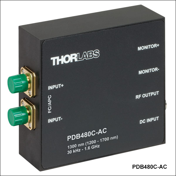
Our highest bandwidth detectors are offered in an AC-coupled version only. The PDB480C-AC, PDB481C-AC, and PDB482C-AC balanced detectors offer bandwidths up to 2.5 GHz, leading to considerable speed improvements. The ultra-low-distortion output stage supports up to a 2 Vp-p A/D card input range, which, combined with the fiber-coupled design, improves the image quality for OCT applications considerably.
Housed in a shielded aluminum enclosure measuring 85 mm x 80 mm x 30 mm, these detectors are post mountable using the included adapter plate, which can be attached to the bottom or side of the housing with the included M2 screws.
PDB835 Series Ultra-Low-Noise, Artifact-Free Detectors (DC - 500 MHz)
The PDB835C and PDB35C-AC detectors feature free-space InGaAs photodiodes connected to FC/APC optical inputs for the 800 - 1700 nm range. Their transimpedance amplifiers feature ultra-low noise over their entire operating bandwidth (up to 500 MHz; see the Specs tab for details on the minimum NEP). These detectors feature FC/APC connectors which are individually aligned to the photodiode and achieve artifact-free operation. Each detector features a compact 76.7 mm x 60.0 mm x 20.0 mm housing with 8-32 (M4 x 0.7) combi-thread mounting holes on the top and bottom sides for universal mounting.
Power Supply
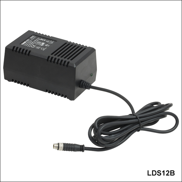
A ±12 V linear power supply that supports input voltages of 100, 120, and 230 VAC is included with each amplified photodetector. Replacement power supplies are available separately below.
A complete list of all of Thorlabs' balanced amplified photodetectors with fast monitor output can be found here. Alternatively, we also offer an APD-based auto-balanced detector with an exceptionally low noise floor suitable for OCT applications with low signal in the sample arm. Thorlabs also offers Fiber-Based Interferometers, which feature an integrated balanced detector.
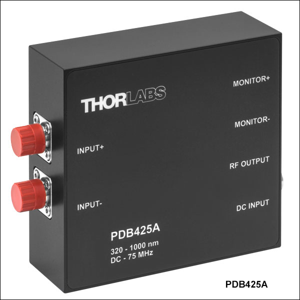
| Item # | PDB415A | PDB415C | PDB425A | PDB425C | PDB440A | PDB440C | PDB465A | PDB465C |
|---|---|---|---|---|---|---|---|---|
| Detector Type | Si/PIN | InGaAs/PIN | Si/PIN | InGaAs/PIN | Si/PIN | InGaAs/PIN | Si/PIN | InGaAs/PIN |
| Wavelength Range | 320 - 1000 nm | 800 - 1700 nm | 320 - 1000 nm | 800 - 1700 nm | 320 - 1000 nm | 800 - 1700 nm | 320 - 1000 nm | 800 - 1700 nm |
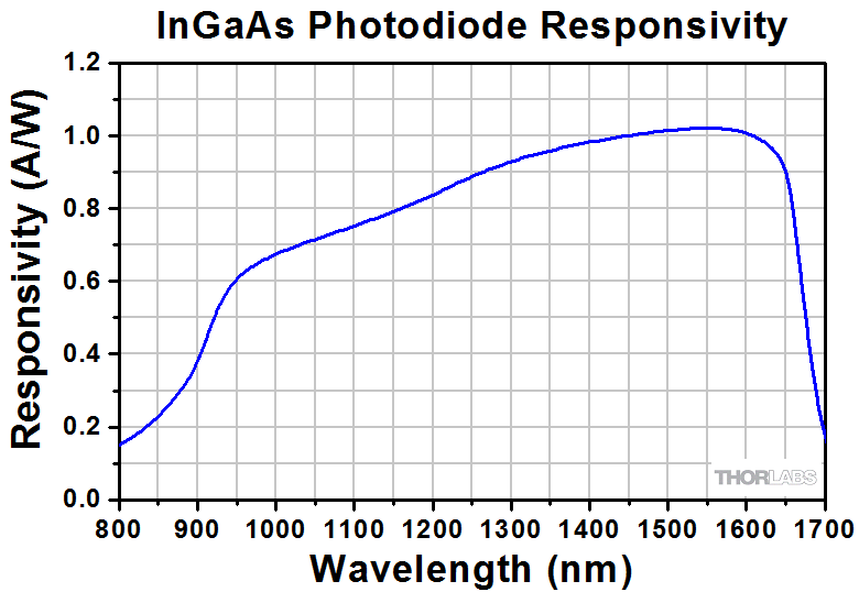
| Typical Max Responsivity | 0.53 A/W | 1.0 A/W | 0.53 A/W | 1.0 A/W | 0.53 A/W | 1.0 A/W | 0.50 A/W | 1.0 A/W |
| Active Detector Diameter | 0.8 mm | 0.3 mm | 0.8 mm | 0.3 mm | 0.8 mm | 0.3 mm | 0.8 mm | 0.15 mm |
| Bandwidth (3 dB) | DC - 100 MHz | DC - 75 MHz | DC - 15 MHz | DC - 200 MHz | ||||
| Common Mode Rejection Ratio |
>25 dB | >35 dB | >35 dB | <25 dB | ||||
| Transimpedance Gaina | 50 x 103 V/A | 250 x 103 V/A | 51 x 103 V/A | 30 x 103 V/A | ||||
| Minimum NEPb | 12.03 pW/Hz1/2 (DC - 100 MHz) |
6.99 pW/Hz1/2 (DC - 100 MHz) |
9.5 pW/Hz1/2 (DC - 75 MHz) |
5.2 pW/Hz1/2 (DC - 75 MHz) |
6.9 pW/Hz1/2 (DC - 15 MHz) |
3.9 pW/Hz1/2 (DC - 15 MHz) |
22.86 pW/Hz1/2 (DC - 200 MHz) |
8.52 pW/Hz1/2 (DC - 200 MHz) |
| RF Output | ||||||||
| RF Output Conversion Gaina,c | 26.5 x 10³ V/W | 50 x 103 V/W | 133 x 103 V/W | 250 x 103 V/W | 27 x 103 V/W | 51 x 103 V/W | 16 x 103 V/W | 30 x 103 V/W |
| CW Saturation Power | 135 µW @ 820 nm |
72 µW @ 1550 nm |
27 µW @ 820 nm |
15 µW @ 1550 nm |
130 µW @ 820 nm |
70 µW @ 1550 nm |
225 µW @ 820 nm | 120 µW @ 1550 nm |
| Impedance | 50 Ω | |||||||
| Max Voltage Swing | ±1.8 V for 50 Ω Load ±3.6 V for High-Impedance Load |
|||||||
| DC Offset | < ±3 mV | |||||||
| RF-Output Coupling | DCd | |||||||
| Monitor Outputs | ||||||||
| Monitor Output Conversion Gain | 10 V/mW @ 820 nm |
10 V/mW @ 1550 nm |
10 V/mW @ 820 nm |
10 V/mW @ 1550 nm |
10 V/mW @ 820 nm |
10 V/mW @ 1550 nm |
10 V/mW @ 820 nm |
10 V/mW @ 1550 nm |
| Impedance | 220 Ω | |||||||
| Max Voltage Swing | 1.55 V for 50 Ω Load 10 V for High-Impedance Load |
|||||||
| Bandwidth | DC to 1 MHz | |||||||
| Voltage Noise | <180 µVRMS | |||||||
| DC Offset | < ±2 mV | |||||||
| General | ||||||||
| Fiber Optical Inputse | FC/PC or FC/APC (Removable) |
FC/PC or FC/APC (Not Removable) |
FC/PC or FC/APC (Removable) |
FC/PC or FC/APC (Not Removable) |
||||
| Photodiode Damage Threshold | 20 mW | |||||||
| Electrical Outputs | SMA (Qty. 3) | |||||||
| Dimensions | 85 mm x 80 mm x 30 mm (3.35" x 3.15" x 1.18") | |||||||
| Weight | 0.35 kg (without Power Supply) | |||||||
| Operating Temperature Rangef | 0 to 40 °C |
|||||||
| Storage Temperature Range | -40 to 70 °C | |||||||
| Included Power Supplyg | ±12 V @ 200 mA 115/230 VAC, 50 - 60 Hz, Switchable |
|||||||
| Item # | PDB470Ca | PDB471Ca | PDB480C-ACa | PDB481C-ACa | PDB482C-ACa | PDB835Ca | PDB835C-ACa |
|---|---|---|---|---|---|---|---|
| Detector | |||||||
| Detector Type | InGaAs/PIN | ||||||
| Optical Inputs | FC/APC | ||||||
| Internal Coupling Fiber | SMF-28e+ | HI1060 | SMF-28e+ | HI1060 | None | ||
| Coupling Loss | <0.5 dB (<0.3 dB Typ.) | <1.0 dB (<0.4 dB Typ.) | <0.5 dB (<0.3 dB Typ.) | <1.0 dB (<0.4 dB Typ.) | N/A | ||
| Operating Wavelength | Optimized for 1300 nm (1200 - 1700 nm Range) |
Optimized for 1060 nm (900 - 1400 nm Range) |
Optimized for 1300 nm (1200 - 1700 nm Range) |
Optimized for 1060 nm (900 - 1400 nm Range) |
800 - 1700 nm | ||
| Responsivity (Typical) | 0.9 A/W @ 1550 nm | 0.72 A/W @ 1060 nm | 0.9 A/W @ 1550 nm | 0.72 A/W @ 1060 nm | 1.0 A/W @ 1550 nm | ||
| Active Detector Diameter | 0.075 mm | 0.080 mm | 0.075 mm | 0.08 mm | |||
| Optical Back Reflection | <-40 dB | N/A | |||||
| Photodiode Damage Threshold | 10 mW | 5 mW | 10 mW | 5 mW | 20 mW | ||
| RF OUTPUT | |||||||
| RF OUTPUT Bandwidth (3 dB) | DC - 400 MHz | 30 kHz - 1.6 GHz | 30 kHz - 1.0 GHz | 1 MHz - 2.5 GHz | DC - 500 MHz | 1 kHz - 500 MHz | |
| Common Mode Rejection Ratio | >25 dB (Typ. >30 dB) | >20 dB (Typ. >25 dB) | >25 dB | ||||
| RF OUTPUT Transimpedance Gain | 10 x 103 V/Ab | 16 x 103 V/Ac | 28 x 103 V/Ac | 10 x 103 V/Ad | |||
| RF OUTPUT Conversion Gain | 9 x 10³ V/W @ 1550 nmb |
7.2 x 10³ V/W @ 1060 nmb |
14.4 x 10³ V/W @ 1550 nmc |
11.5 x 10³ V/W @ 1060 nmc |
20 x 103 V/W @ 1060 nmc |
10 x 103 V/W @ 1550 nmd,e | |
| RF OUTPUT Power at 1 dB Compressionc |
- | +16.5 dBm Min+18 dBm Typ. | - | ||||
| RF OUTPUT CW Saturation Power | 420 µW @ 1550 nm | 530 µW @ 1060 nm | See Note Below | 360 mW @ 1550 nm | |||
| RF OUTPUT Coupling | DC (AC Coupling Available upon Request) | AC Coupling Only | DC | AC | |||
| RF OUTPUT Impedance | 50 Ω | ||||||
| Max Voltage Swing | ±1.9 V for 50 Ω Load ±3.8 V for High-Z Load |
See Note Below | ±1.8 V for 50 Ω Load; ±3.6 V (Linear Over 0 to 2.5 V) for High-Z Load |
||||
| Minimum NEPf | 8 pW/Hz1/2 (DC to 100 MHz) |
9.3 pW/Hz1/2 (30 kHz to 100 MHz) |
9.0 pW/Hz1/2 (30 kHz to 100 MHz) |
12.0 pW/Hz1/2 (1 MHz to 100 MHz) |
6.5 pW/Hz1/2 (DC to 500 MHz) |
||
| Overal Output Voltage Noise | <2.0 mVRMS | <9 mVRMS | <6.5 mVRMS | <12 mVRMS | <1.5 mVRMS | ||
| DC Offset | N/A | < ±5 mV | |||||
| MONITOR Outputs | |||||||
| MONITOR Output Impedance | 200 Ω | ||||||
| MONITOR Output Bandwidth (3 dB) | DC - 3 MHz | DC - 2.5 MHz | DC - 1 MHz | ||||
| MONITOR Output Conversion Gain, High Z Loadb |
9 V/mW @ 1550 nm | 7.2 V/mW @ 1060 nm | 9 V/mW @ 1550 nm | 7.2 V/mW @ 1060 nm | 10 V/mW @ 1550 nme | ||
| MONITOR Output Voltage Swing | 10 V Max, High-Z Load | 1.5 V Max for 50 Ω Load 10 V Max (Linear Over 0 to 5 V) for High-Z Load |
|||||
| Overall Output Voltage Noise | <0.65 mVRMS | <0.6 mVRMS | |||||
| DC Offset | < ±2 mV | < ±5 mV | |||||
| General | |||||||
| Electrical Outputs | SMA | ||||||
| Included DC Power Supplyg | ±12 V @ 250 mA 100/120/230 VAC, 50 - 60 Hz, Switchable |
||||||
| Operating Temperature Rangeh | 0 °C to 40 °C | ||||||
| Storage Temperature Range | -40 °C to 70 °C | ||||||
| Dimensions (W x H x D) | 85 mm x 80 mm x 30 mm (3.35" x 3.15" x 1.18") |
76.7 mm x 60.0 mm x 20.0 mm (3.02" x 2.36" x 0.79") |
|||||
| Weight | 0.35 kg | 0.13 kg | |||||
Note:
For the PDB480C-AC, PDB481C-AC, and PDB482C-AC detectors the RF output signal must not exceed the RF Output Power at 1 dB Compression, which is the point at which the amplified signal at 1 GHz is compressed by 1 dB. Above this value, the amplified signal will become non-linear and begin to saturate. The RF output voltage at this saturation point can be calculated using the following formula:
![]()
where R is the load impedance (50 Ω), P0 is defined as 1 mW, and L(dBm) is the power level in dBm. Using the specified RF Output Power at 1 dB Compression of 16.5 dBm, this yields the following "maximum" output voltage:

Operation of Balanced Detectors with Bandwidths up to 500 MHz
Thorlabs' Balanced Amplified Photodetectors consist of two well-matched photodiodes and an ultra-low noise, high-speed transimpedance amplifier (TIA) that generates an output voltage (RF OUTPUT) proportional to the difference between the photocurrents in the two photodiodes (i.e., the two optical input signals). Additionally, the unit has two fast monitor outputs (MONITOR+ and MONITOR-) to observe the optical input power levels on each photodiode separately. These outputs are low frequency outputs and cannot be used to measure an RF modulation on the signal. The block diagram applies to our balanced detectors with bandwidths up to 500 MHz.
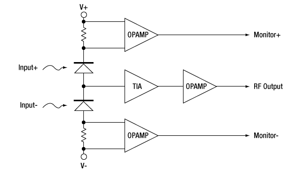
Figure 3.1 Block Diagram of a Circuit with balanced detectors with bandwidths up to 500 MHz.
Operation of the PDB480C-AC, PDB481C-AC, and PDB482C-AC Balanced Detectors
The PDB48xC-AC Balanced Amplified Photodetectors use the same basic operating principles as described above and have the following additional features. The TIA's ultra-low distortion output stage supports up to a 2 Vp-p A/D card input range. The two fast monitor outputs can be used to measure not only the individual optical input power levels, but also low frequency modulated signals up to 3 MHz (Item #s PDB480C-AC and PDB481C-AC) or 2.5 MHz (Item # PDB482C-AC). To enable the much higher frequency of these detectors, the photodiodes are connected to the inputs with length-matched fibers, only AC-coupled versions are offered, and capacitors are added to the circuit (as shown in Figure 3.2).
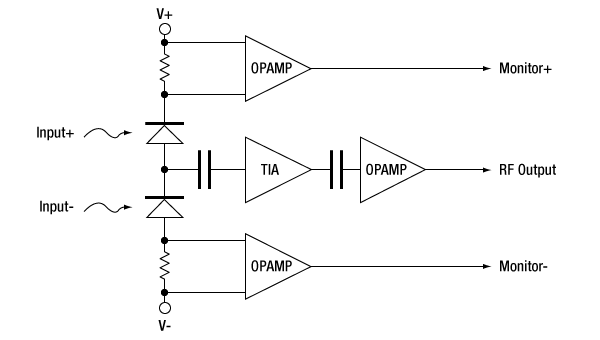
Figure 3.2 Block Diagram of a Circuit with balanced detectors and added capacitors.
Pin Diagrams for OCT Balanced Detectors
Monitor +/-
SMA Female
Maximum Voltage is +10 V for Hi-Z & +1.5 V into 50 Ω loads.
RF Output
SMA Female
For the PDB415, PDB425, PDB440, PDB465, and PDB835 photodetectors, the max RF OUTPUT voltage is ±3.6 V for Hi-Z & ±1.8 V into 50 Ω loads.
The RF OUTPUT CW saturation power is 420 µW @ 1550 nm and 530 µW at 1060 nm for the PDB470C and PDB471C, respectively.
For the PDB48xC-AC photodetectors, the RF OUTPUT Power at 1 dB compression into 50 Ω loads is +16.5 dBm (Min), +18 dBm (Typical)
PDB Male (Power Cables)

PDB Female (Photodetector)

| Posted Comments: | |
议焕 施
(posted 2025-09-02 04:37:32.63) 你好,我们购买了您们PDB480C-AC的PD,有一个通道可能烧了,请问这个可以维修吗? sacosta
(posted 2025-09-03 08:26:31.0) Thanks for reaching out, we will contact you directly to troubleshoot. Markus Schmidt
(posted 2021-06-19 23:06:57.393) Hello
I read PDB470C Manual. As I know for some Photodetectors, the bandwidth has relation with R_load. Is it right for PDB470C?
for example if I add a 50 Ohm or 1 M Ohm R_load, what will be the photodetector bandwidth?
Regards soswald
(posted 2021-06-28 08:51:07.0) Dear Markus,
thank you for your feedback. The bandwidth of the PDB470C does not vary with the terminating load.
We recommend a 50 Ohm load for the RF output and Hi-Z for the Monitor outputs. sebastian.marschall
(posted 2013-09-23 13:17:20.217) Hello
What is the reason for the different frequency responses of the PDB480C-AC (1.6 GHz) and the PDB481C-AC (1.0 GHz).
Would there be big problems when using the PDB480C-AC with 1060 nm light (coupling losses, mode-dispersion, etc.)?
Regards, Sebastian tschalk
(posted 2013-09-26 06:29:00.0) This is a response from Thomas at Thorlabs. Thank you very much for your inquiry. The bandwidth of the respective detector is defined by the pigtailed diodes built in. Those are designed for a specific wavelength, both because of the fiber used as pigtail as well as for the diode itself. The diode used in the PDB481-AC can unfortunately operate in a stable regime only up to 1GHz. While it would be in principle be possible to use the PDB480C-AC at 1060nm, the diode being not optimized for this wavelength would induce higher losses. The modal dispersion in this case should be negligible considering the short length of the pigtails. I will contact you directly with more detailed information. |

 Zoom
Zoom| Specificationsa | ||||||
|---|---|---|---|---|---|---|
| Item # | PDB440A | PDB425A | PDB415A | PDB465A | ||
| Wavelength Range | 320 - 1000 nm | |||||
| Detector Type | Si/Pin | |||||
| Typical Max Responsivity (Click for Plot) |
0.53 A/W | 0.50 A/W | ||||
| Active Detector Diameter | 0.8 mm | |||||
| Bandwidth (3 dB) | DC - 15 MHz | DC - 75 MHz | DC - 100 MHz | DC - 200 MHz | ||
| Common Mode Rejection Ratio | >35 dB | >25 dB | ||||
| Transimpedance Gainb | 51 x 103 V/A | 250 x 103 V/A | 50 x 103 V/A | 30 x 103 V/A | ||
| Minimum NEP | 6.9 pW/Hz1/2 (DC - 15 MHz) |
9.5 pW/Hz1/2 (DC - 75 MHz) |
12.03 pW/Hz1/2 (DC - 100 MHz) |
22.86 pW/Hz1/2 (DC - 200 MHz) |
||
| Optical Inputs | FC/PC or FC/APC (Removable) | |||||
| Monitor Output Bandwidth | DC - 1 MHz | |||||

 Zoom
Zoom| Specificationsa | ||||||
|---|---|---|---|---|---|---|
| Item # | PDB440C | PDB425C | PDB415C | PDB465C | PDB835Cb | PDB835C-ACb |
| Wavelength Range | 800 - 1700 nm | |||||
| Detector Type | InGaAs/PIN | |||||
| Typical Max Responsivity (Click for Plot) |
1.0 A/W | |||||
| Active Detector Diameter | 0.3 mm | 0.15 mm | 0.08 mm | |||
| Bandwidth (3 dB) | DC - 15 MHz | DC - 75 MHz | DC - 100 MHz | DC - 200 MHz | DC - 500 MHz | 1 kHz - 500 MHz |
| Common Mode Rejection Ratio | >35 dB | >25 dB | ||||
| Transimpedance Gainc | 51 x 103 V/A | 250 x 103 V/A | 50 x 103 V/A | 30 x 103 V/A | 10 x 103 V/A @ 1550 nm | |
| Minimum NEP | 3.9 pW/Hz1/2 (DC - 15 MHz) |
5.2 pW/Hz1/2 (DC - 75 MHz) |
6.99 pW/Hz1/2 (DC - 100 MHz) |
8.52 pW/Hz1/2 (DC - 200 MHz) |
6.5 pW/Hz1/2 (DC to 500 MHz) |
|
| Optical Inputs | FC/PC or FC/APC (Removable) |
FC/PC or FC/APC (Not Removable) |
FC/APC (Not Removable) |
|||
| Monitor Output Bandwidth | DC - 1 MHz | |||||

 Zoom
Zoom| Specificationsa | |||
|---|---|---|---|
| Item # | PDB471C | PDB481C-AC | PDB482C-AC |
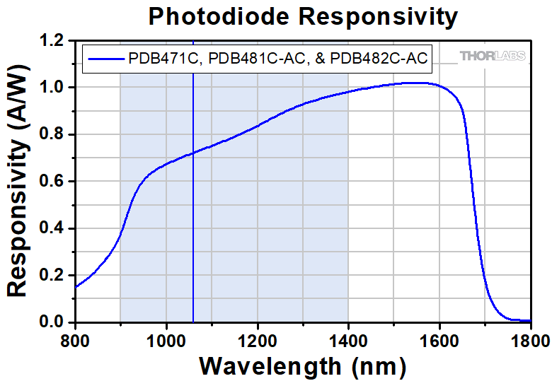
| Operating Wavelength | Optimized for 1060 nm (900 - 1400 nm Range) | ||
| Detector Type | InGaAs/PIN | ||
| Internal Coupling Fiber | HI1060 | ||
| Typical Responsivity (Click for Plot) |
0.72 A/W @ 1060 nm | ||
| Active Detector Diameter | 0.080 mm | ||
| Bandwidth (3 dB) | DC - 400 MHz | 30 kHz - 1.0 GHz | 1 MHz - 2.5 GHz |
| Common Mode Rejection Ratio | >25 dB (Typ. >30 dB) | >20 dB (Typ. >25 dB) | |
| Transimpedance Gain | 10 x 103 V/Ab | 16 x 103 V/Ac | 28 x 103 V/Ac |
| Minimum NEP | 8 pW/Hz1/2 (DC - 100 MHz) |
9.0 pW/Hz1/2 (30 kHz - 100 MHz) |
12.0 pW/Hz1/2 (1 MHz - 100 MHz) |
| Optical Inputs | FC/APC | ||
| Monitor Output Bandwidth | DC - 3 MHz | DC - 2.5 MHz | |

 Zoom
Zoom| Specificationsa | ||||
|---|---|---|---|---|
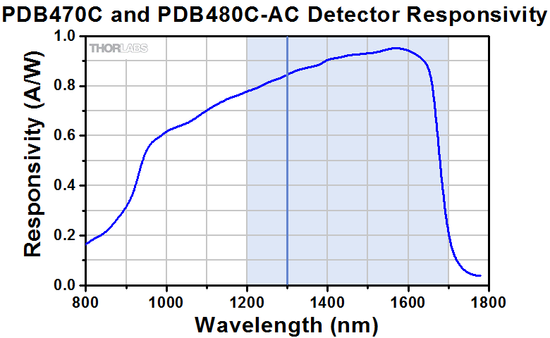
| Item # | PDB470C | PDB480C-AC | ||
| Operating Wavelength | Optimized for 1300 nm (1200 - 1700 nm Range) | |||
| Detector Type | InGaAs/PIN | |||
| Internal Coupling Fiber | SMF-28e+ | |||
| Typical Responsivity (Click for Plot) |
0.9 A/W @ 1550 nm | |||
| Active Detector Diameter | 0.075 mm | |||
| Bandwidth (3 dB) | DC - 400 MHz | 30 kHz - 1.6 GHz | ||
| Common Mode Rejection Ratio | >25 dB (Typ. >30 dB) | |||
| Transimpedance Gain | 10 x 103 V/Ab | 16 x 103 V/Ac | ||
| Minimum NEP | 8 pW/Hz1/2 (DC - 100 MHz) |
9.3 pW/Hz1/2 (30 kHz - 100 MHz) |
||
| Optical Inputs | FC/APC | |||
| Monitor Output Bandwidth | DC - 3 MHz | |||

 Zoom
Zoom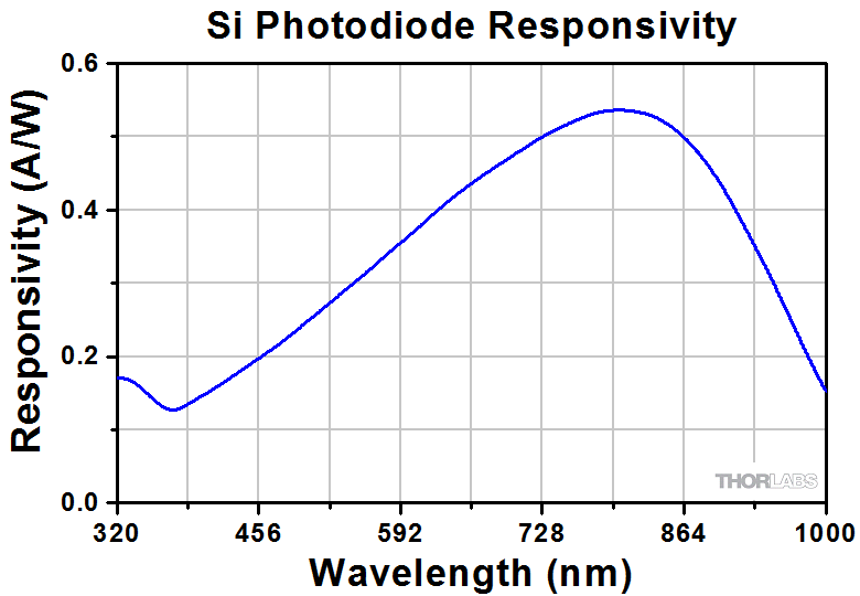
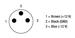 Figure 508A LDS12B Male Power Cable
- Replacement Power Supply for the Balanced Amplified Photodetectors Sold Above
- ±12 VDC Power Output
- Current Limit Enabling Short Circuit and Overload Protection
- On/Off Switch with LED Indicator
- Switchable AC Input Voltage (100, 120, or 230 VAC)
- 2 m (6.6') Cable with LUMBERG RSMV3 Male Connector
- UL and CE Compliant
The LDS12B ±12 VDC Regulated Linear Power Supply is intended as a replacement for the supply included with our PDB line of balanced photodetectors sold on this page. The cord has three pins: one for ground, one for +12 V, and one for -12 V (see Figure 508A). A region-specific power cord is shipped with the unit based on your location. This power supply can also be used with the PDA series of amplified photodetectors, PMM series of photomultiplier modules, APD series of avalanche photodetectors, and the FSAC autocorrelator for femtosecond lasers.