 Products Home / Polarization Optics / Liquid Crystal Devices / Half-Wave Liquid Crystal Variable Retarders / Wave Plates
Half-Wave Liquid Crystal Variable Retarders / Wave Plates
- Nematic Liquid Crystal Half-Wave Variable Retarders
- Available with Ø10 mm or Ø20 mm Clear Aperture
- AR Coated for Visible, NIR, or MIR Light
- Compensated Models Achieve 0 nm Retardance
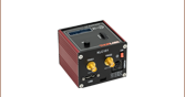
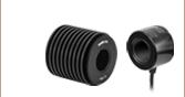
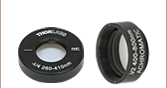
LCC1221-B
Ø20 mm Clear Aperture,
<20 ms Switching Time,
Mounted, Uncompensated
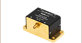
LCC1611-C
Ø10 mm Clear Aperture,
<23 ms Switching Time,
Mounted, Compensated
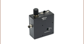
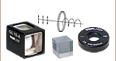
LCC25
Benchtop LC Controller
LCC1421-A
Ø20 mm Clear Aperture,
<17 ms Switching Time,
Mounted, Compensated
KLC101
K-Cube™ LC Controller
LCC1111U-A
Ø10 mm Clear Aperture,
<11 ms Switching Time,
Unmounted, Uncompensated


Please Wait
Operating Principle
High Retardance
Low Retardance
Figure 1: In their nematic phase, liquid crystal molecules have an ordered orientation, which together with the stretched shape of the molecules creates an optical anisotropy. When an electric field is applied, the molecules align to the field and the level of birefringence is controlled by the tilting of the LC molecules.
Compensating for Residual Retardance

Click to Enlarge
Uncompensated LC Retarder
Click to Enlarge
Compensated LC Retarder
Figure 2: The minimum retardation of uncompensated liquid crystal retarders is ~30 nm. Our compensated LC retarders include a liquid crystal polymer compensator with a fixed retardation and slow axis that is orthogonal to that of the variable LC cell. This enables our compensated retarders to achieve a minimum retardance of 0 nm.
| Selection Guide for LC Retarders | |
|---|---|
| Type | Clear Aperture |
| Half Wave | Ø10 mm or Ø20 mm |
| Half Wave, Thermally Stabilized | Ø10 mm |
| Full Wave | Ø10 mm or Ø20 mm |
| Full Wave, Thermally Stabilized | Ø20 mm |
| Multi-Wave | Ø10 mm |
| Multi-Wave, Integrated Controller | Ø10 mm |
| Custom LC Retarders | |
Features
- Variable Wave Plate to Actively Control the Polarization State and/or Phase Delay of Light
- Retardance Range:
- 0 nm to λ/2 for LC Retarders with Residual Retardance Compensation
- ~30 nm to λ/2 for Uncompensated LC Retarders
- Clear Aperture: Ø10 mm or Ø20 mm
- Ø10 mm Aperture Available in Mounted or Unmounted Packages
- Fast Switching Ø10 mm Retarders with Rise + Fall Times as Low as ~3 ms at 25 °C
- Highly Uniform Retardance Over Entire Clear Aperture (See Specs Tab for Details)
- Compatible with Our LCC25 and KLC101 Voltage Controllers (Sold Separately Below)
Thorlabs' Half-Wave Liquid Crystal Variable Retarders (LCVR) use a nematic liquid crystal cell to function as a variable wave plate. The absence of moving parts provides quick switching times on the order of milliseconds (see the Switching Time tab for details). AR coatings are available for five wavelength ranges: 350 - 700 nm, 650 - 1050 nm, 1050 - 1700 nm, 1650 - 3000 nm, or 3600 - 5600 nm (see the Performance tab for transmission and retardance data).
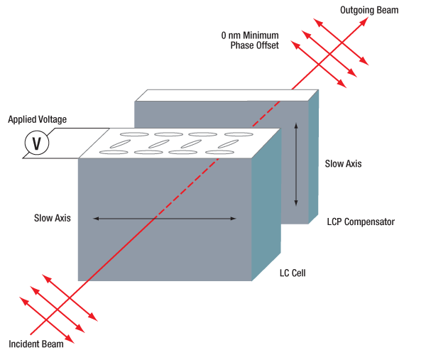
Thorlabs offers Ø10 mm and Ø20 mm clear aperture sizes. Both sizes are available in one of two variable retardation ranges: 0 nm to λ/2 retardation for retarders with residual retardance compensation, and ~30 nm to λ/2 retardation for uncompensated LC retarders. Our compensated retarders integrate a phase compensator made of liquid crystal polymers, which compensate the residual retardation of the LCVR to achieve true zero retardation at a specific driving voltage (see the Performance tab for more information). Its structure and principle are described to the right.
Our mounted Ø10 mm clear aperture retarders feature a 1" outer diameter housing, making them compatible with our Ø1" optics mounts. Additionally, we offer Ø10 mm clear aperture retarders that are unmounted for OEM and other specialized applications. Our Ø20 mm retarders have a 2" outer diameter, providing compatibility with our Ø2" optics mounts. Please refer to the Specs tab for suggested compatible mounts.
Performance
These liquid crystal variable retarders provide excellent uniformity, low optical losses, and low wavefront distortion. Our retarders also provide a quick switching time, a broad operating temperature range, and a wide wavelength range. Please see the Specs, Performance, and Switching Time tabs for complete details. We also offer temperature-stabilized half-wave retarders for increased long-term stability.
Fast Switching Ø10 mm Retarders
The Ø10.0 mm clear aperture LCC1511-x uncompensated and LCC1611-x compensated LCVRs feature a nematic liquid crystal variant that results in switching times more than three times faster than the LCC1111-D, LCC1111-MIR, and Ø20 mm LCVRs.
Previous Generation Ø10 mm Retarders
If your application doesn't require the fast switching speeds of the LCC1511-x and LCC1611-x LCVRs, the previous generation Ø10 mm clear aperture retarders that share the same specifications and use the same nematic liquid crystal as the Ø20 mm LCVRs are available upon request by contacting Tech Sales. See the Custom Capabilities tab for details.
Operation
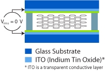
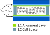
As illustrated in Figure 1, a Liquid Crystal Variable Retarder consists of a transparent cell filled with a solution of Liquid Crystal (LC) molecules and functions as a variable wave plate. The orientation of the LC molecules is determined by the alignment layer in the absence of an applied voltage. The alignment layer is composed of an organic polyimide (PI) coating whose molecules are aligned in the rubbing direction during manufacturing. Due to the birefringence of the LC material, this LC retarder acts as an optically anisotropic wave plate, with its slow axis, marked on the mechanical housing, parallel to the surface of the retarder. Two parallel inner faces of the cell wall are coated with a transparent conductive film so that a voltage can be applied across the cell. When an AC voltage is applied, the LC molecules will reorient from their default alignment according to the applied Root-Mean-Square voltage (VRMS). Hence, a varying applied voltage can actively control the retardance of the liquid crystal variable retarder.
Residual Retardation Compensation
Due to the surface anchoring of the PI layer, even when a voltage is being applied, there are still some liquid crystal molecules that cannot be reoriented, especially near the alignment layers. This results in the residual retardation of the LC retarder during operation. Thorlabs' uncompensated LC retarders have ~30 nm residual retardation at 25 VRMS driving voltage, as depicted in Figure 2 above. To meet the need for true zero retardation in sensitive applications, we offer the compensated LC retarders. A compensating layer made of liquid crystal polymer (LCP) is bonded on the LC cell, with its slow axis perpendicular to that of the LC cell. The fixed retardation of LCP compensator is ~50 nm. Thus, at a specific driving voltage between 5 V and 20 V, the retardation of the LC cell and the compensator cancel each other, resulting in true zero retardation. This comes at a cost of slightly degraded retardation uniformity and higher overall thickness. See the Specs and Performance tabs for more information.
Controllers
The LCC25 and KLC101 liquid crystal controllers provide active DC offset compensation while applying an AC voltage (0 to 25 VRMS). The DC offset compensation automatically zeros the DC bias across the LC device in order to counteract the buildup of charge.
Compensated Half-Wave LC Retarders
| Item # | LCC1611-A | LCC1421-A | LCC1611-B | LCC1421-B | LCC1611-C | LCC1421-C | |
|---|---|---|---|---|---|---|---|
| Wavelength Range | 350 - 700 nma | 650 - 1050 nm | 1050 - 1700 nm | ||||
| Retardance Rangeb | 0 nm to >λ/2 | ||||||
| Clear Aperture | Ø10 mm | Ø20 mm | Ø10 mm | Ø20 mm | Ø10 mm | Ø20 mm | |
| Housing Outer Dimensions | Ø1"c (Ø25.4 mm) |
Ø2.20"d (Ø55.8 mm) |
Ø1"c (Ø25.4 mm) |
Ø2.20"d (Ø55.8 mm) |
Ø1"c (Ø25.4 mm) |
Ø2.20"d (Ø55.8 mm) |
|
| Liquid Crystal Material | Nematic Liquid Crystal | ||||||
| Surface Quality | 60-40 Scratch-Dig | ||||||
| Parallelism | <5 arcmin | ||||||
| Switching Time (Rise/Fall, Typical)e |
3.34 ms / 0.14 ms @ 25 °C, 635 nm |
15.8 ms / 260 µs @ 22 °C, 635 nm |
4.01 ms / 0.27 ms @ 25 °C, 780 nm |
34.0 ms / 360 µs @ 22 °C, 780 nm |
22.34 ms / 0.55 ms @ 25 °C, 1550 nm |
152 ms / 510 µs @ 25.6 °C, 1550 nm |
|
| Operating Voltage (Max)f | 25 V | ||||||
| Damage Threshold |
Pulsed (ns) | 1.0 J/cm2 (532 nm, 10 Hz, 8 ns, Ø200 µm) |
1.7 J/cm2 (810 nm, 10 Hz, 7.6 ns, Ø234 µm) |
1.2 J/cm2 (1542 nm, 10 Hz, 10 ns, Ø458 µm) |
|||
| Pulsed (fs) | 0.01 J/cm2 (532 nm, 100 Hz, 76 fs, Ø162 µm) |
0.01 J/cm2 (800 nm, 100 Hz, 36.4 fs, Ø189 µm) |
0.08 J/cm2 (1550 nm, 100 Hz, 70 fs, Ø145 µm) |
||||
| AR Coatingg | Ravg < 0.5% | ||||||
| Wavefront Distortion | ≤λ/4 @ 635 nm | ||||||
| Retardance Uniformity (RMS)h | <λ/20 @ 400 nm | <λ/20 @ 650 nm | <λ/20 @ 1050 nm | ||||
| Housing Thickness | 8.6 mm (0.34") | 15.0 mm (0.59") | 8.6 mm (0.34") | 15.0 mm (0.59") | 8.6 mm (0.34") | 15.0 mm (0.59") | |
| Storage Temperature | -30 to 70 °C | ||||||
| Operation Temperature | -20 to 45 °C | ||||||
Uncompensated Half-Wave LC Retarders
| Item # | LCC1111U-A | LCC1511-A | LCC1221-A | LCC1111U-B | LCC1511-B | LCC1221-B | |
|---|---|---|---|---|---|---|---|
| Wavelength Range | 350 - 700 nma | 650 - 1050 nm | |||||
| Retardance Rangeb | ~30 nm to >λ/2 | ||||||
| Clear Aperture | Ø10 mm | Ø10 mm | Ø20 mm | Ø10 mm | Ø10 mm | Ø20 mm | |
| Housing Outer Dimensions |
17.0 mm × 12.0 mm (0.67" × 0.47") |
Ø1"c (Ø25.4 mm) |
Ø2"d (Ø50.8 mm) |
17.0 mm x 12.0 mm (0.67" x 0.47") |
Ø1"c (Ø25.4 mm) |
Ø2"d (Ø50.8 mm) |
|
| Liquid Crystal Material | Nematic Liquid Crystal | ||||||
| Surface Quality | 40-20 Scratch-Dig | ||||||
| Parallelism | <5 arcmin | ||||||
| Switching Time (Rise/Fall, Typical)e |
10.2 ms / 310 µs @ 22 °C, 635 nm |
2.72 ms / 0.16 ms @ 25 °C, 635 nm |
10.2 ms / 310 µs @ 22 °C, 635 nm |
19.52 ms / 0.44 ms @ 25 °C, 780 nm |
3.41 ms / 0.24 ms @ 25 °C, 780 nm |
19.52 ms / 0.44 ms @ 25 °C, 780 nm |
|
| Operating Voltage (Max)f | 25 V | ||||||
| Damage Threshold |
Pulsed (ns) | 1.0 J/cm2 (532 nm, 10 Hz, 8 ns, Ø200 µm) |
1.7 J/cm2 (810 nm, 10 Hz, 7.6 ns, Ø234 µm) |
||||
| Pulsed (fs) | 0.01 J/cm2 (532 nm, 100 Hz, 76 fs, Ø162 µm) |
0.01 J/cm2 (800 nm, 100 Hz, 36.4 fs, Ø189 µm) |
|||||
| AR Coatingg | Ravg < 0.5% | ||||||
| Wavefront Distortion | ≤λ/4 @ 635 nm | ||||||
| Retardance Uniformity (RMS)h |
<λ/50 @ 400 nm | <λ/50 @ 650 nm | |||||
| Housing Dimensional Tolerance | ±0.4 mm | - | ±0.4 mm | - | |||
| Housing Thickness | 6.0 mm (0.24") | 8.0 mm (0.32") | 13.0 mm (0.51") | 6.0 mm (0.24") | 8.0 mm (0.32") | 13.0 mm (0.51") | |
| Storage Temperature | -30 to 70 °C | ||||||
| Operation Temperature | -20 to 45 °C | ||||||
| Item # | LCC1511-C | LCC1221-C | LCC1111-D | LCC1111-MIR | |
|---|---|---|---|---|---|
| Wavelength Range | 1050 - 1700 nm | 1650 - 3000 nm | 3600 - 5600 nm | ||
| Retardance Rangea | ~30 nm to >λ/2 | ~30 nm to >λ/2 | ~30 nm to >λ/2 | ~30 nm to >λ/2 | |
| Clear Aperture | Ø10 mm | Ø20 mm | Ø10 mm | Ø10 mm | |
| Housing Outer Dimensions |
Ø1"b (Ø25.4 mm) |
Ø2"c (Ø50.8 mm) |
Ø1"b (Ø25.4 mm) |
Ø1"b (Ø25.4 mm) |
|
| Liquid Crystal Material | Nematic Liquid Crystal | ||||
| Surface Quality | 40-20 Scratch-Dig | 60-40 Scratch-Dig | |||
| Parallelism | <5 arcmin | ||||
| Switching Time (Rise/Fall, Typical)d |
21.29 ms / 0.50 ms @ 25 °C, 1550 nm |
95.8 ms / 1.81 ms @ 25.6 °C, 1550 nm |
192 ms / 1 ms @ 25.6 °C, 2200 nm |
372 ms / 14 ms @ 25.6 °C, 4400 nm |
|
| Operating Voltage (Max)e | 25 V | ||||
| Damage Threshold |
Pulsed (ns) | 1.2 J/cm2 (1542 nm, 10 Hz, 10 ns, Ø458 µm) |
0.041 J/cm2 (2000 nm, 10 Hz, 6.5 ns, Ø292 µm) |
N/A | |
| Pulsed (fs) | 0.08 J/cm2 (1550 nm, 100 Hz, 70 fs, Ø145 µm) |
0.025 J/cm2 (2000 nm, 100 Hz, 100 fs, Ø220 µm) |
N/A | ||
| AR Coatingf | Ravg < 0.5% | Ravg < 1.0% | |||
| Wavefront Distortion | ≤λ/4 @ 635 nm | - | |||
| Retardance Uniformity (RMS)g |
<λ/50 @ 1050 nm | <λ/30 @ 1650 nm | <λ/10 @ 3600 nm | ||
| Housing Thickness | 8.0 mm (0.32") | 13.0 mm (0.51") | 8.0 mm (0.32") | 8.0 mm (0.32") | |
| Storage Temperature | -30 to 70 °C | ||||
| Operation Temperature | -20 to 45 °C | ||||
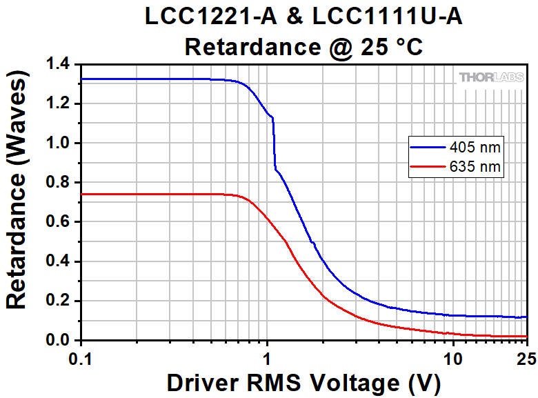
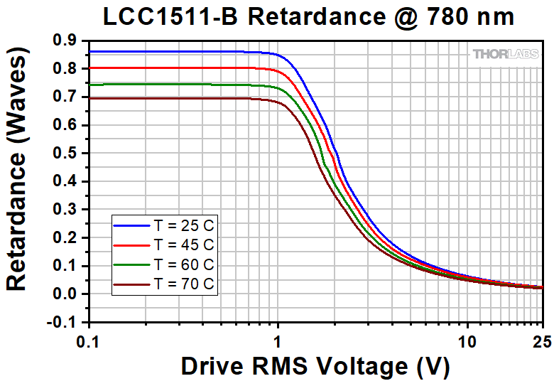
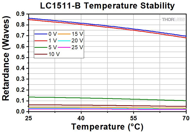
| Variable Half-Wave Retarder Performance Graphs | |||||
|---|---|---|---|---|---|
| Item #a | Wavelength Range | Retardance @ 25 °C |
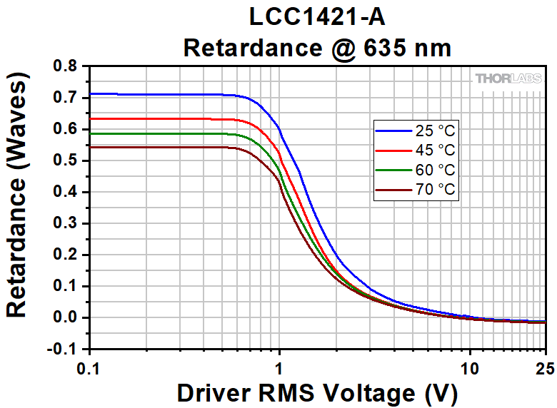
Retardance vs. Temperature |
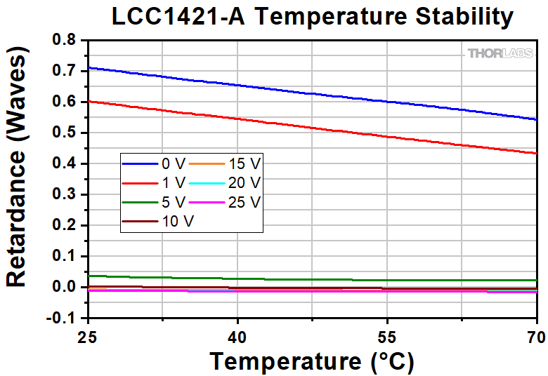
Temperature Stability |
Transmission |
| LCC1611-A | 350 - 700 nm | 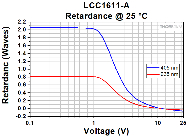 |
 (635 nm) (635 nm) |
 |
|
| LCC1511-A | 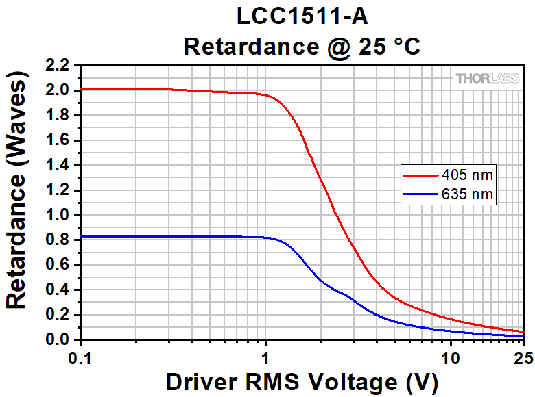 |
 (635 nm) (635 nm) |
 |
||
| LCC1421-A | 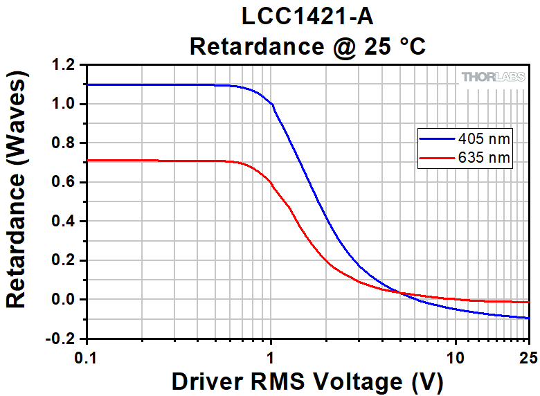 |
 (635 nm) (635 nm) |
 |
||
| LCC1221-A, LCC1111U-A |
 |
 (635 nm) (635 nm) |
 |
||
| LCC1611-B |
650 - 1050 nm | 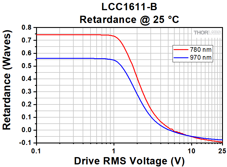 |
 (780 nm) (780 nm) |
 |
|
| LCC1511-B | 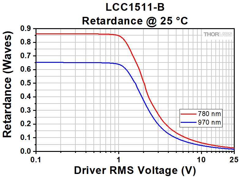 |
 (780 nm) (780 nm) |
 |
||
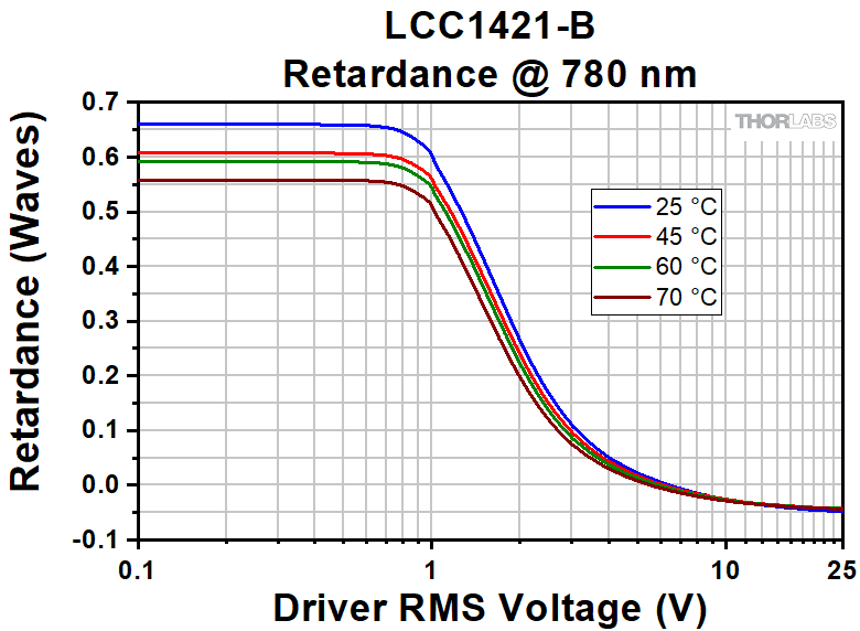
| LCC1421-B | 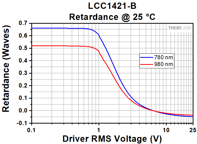 |
 (780 nm) (780 nm) |
 |
||
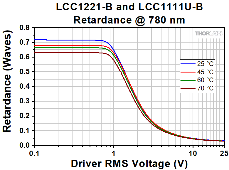
| LCC1221-B, LCC1111U-B |
 |
 (780 nm) (780 nm) |
 |
||
| LCC1611-C |
1050 - 1700 nm | 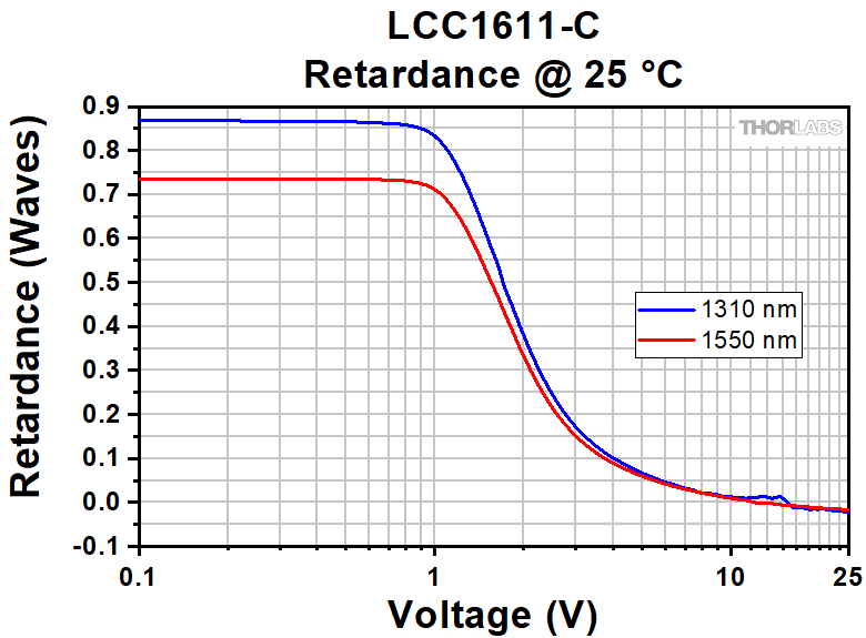 |
 (1550 nm) (1550 nm) |
 |
|
| LCC1511-C | 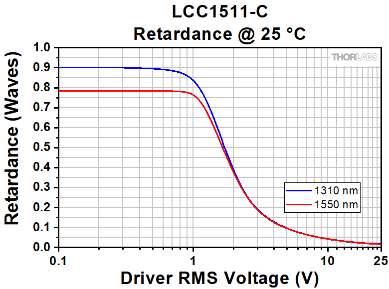 |
 (1550 nm) (1550 nm) |
 |
||
| LCC1421-C | 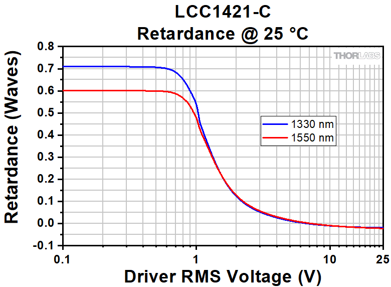 |
 (1550 nm) (1550 nm) |
 |
||
| LCC1221-C |  |
 (1550 nm) (1550 nm) |
 |
||
| LCC1111-D | 1650 - 3000 nm | 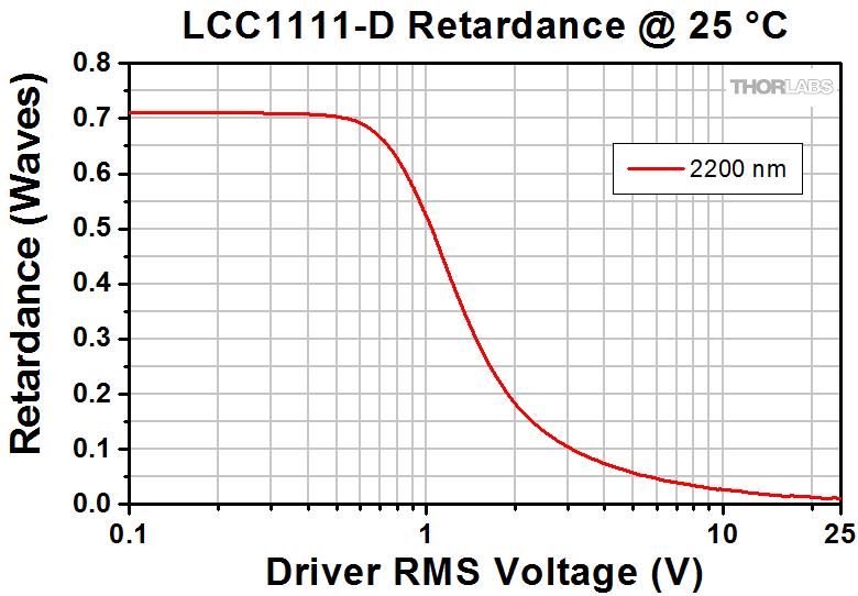 |
 (2200 nm) (2200 nm) |
 |
|
| LCC1111-MIR | 3600 - 5600 nm | 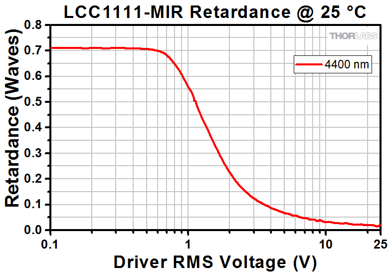 |
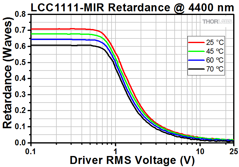 (4400 nm) (4400 nm) |
 |
|
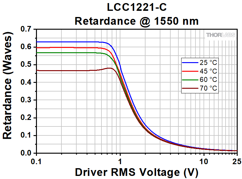
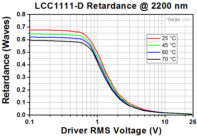
LC Retarder Performance
In their nematic phase, liquid crystal molecules have an ordered orientation, which together with the stretched shape of the molecules, creates an optical anisotropy. When an electric field is applied, the molecules align to the field and the level of effective retardance is controlled by the tilting of the LC molecules. To minimize effects due to ions in the material, an LC device must be driven using an alternating voltage. Our LCC25 and KLC101 controllers, sold below, are designed to minimize the DC bias in the driving signal in the operating range of 0 V to 25 V.
Due to changes in the molecular polarizability, the LC material exhibits higher chromatic dispersion at short wavelengths and comparably small chromatic dispersion at long wavelengths. To account for this, we provide the retardance data at one or two select wavelengths within the product's wavelength range in the table to the right.
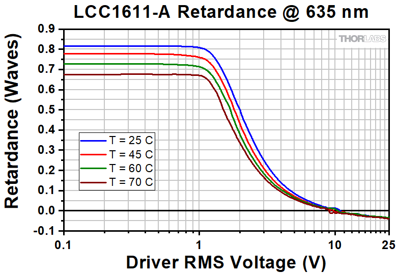
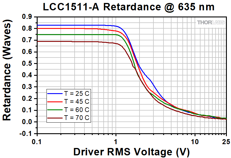
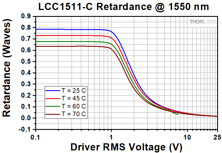
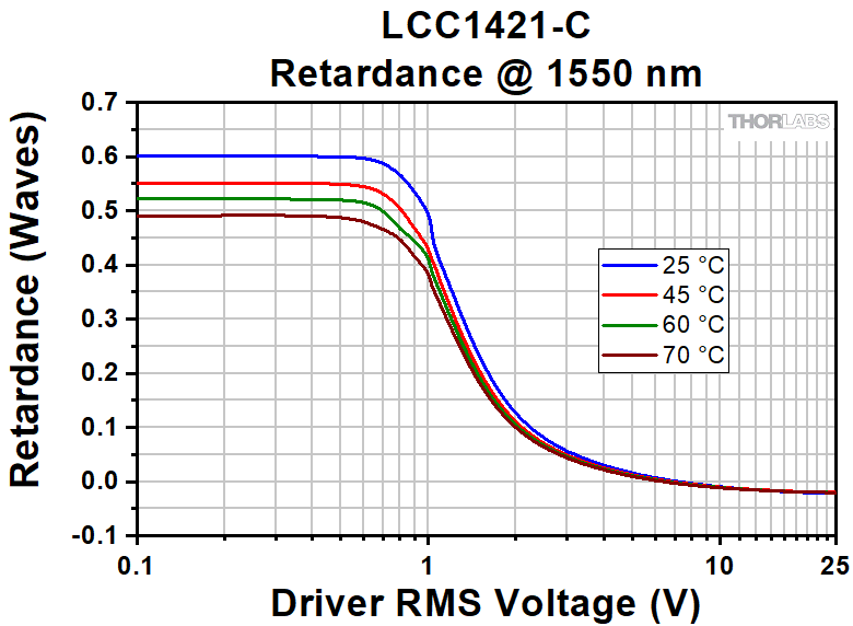
Additionally, the LC retardation also depends on the temperature of the device. As temperature increases, the retardation decreases with it. However, as seen in the Switching Time tab, the switching speed of the LC improves at higher temperatures. Generally, the LC's refractive indices (both ordinary and extraordinary) change more drastically as temperature nears the LC's clearing temperature. As such, we choose to use materials with a high clearing temperature to minimize the temperature dependence when used at room temperature.
LCC1611 and LCC1511 Fast Switching Ø10 mm Clear Aperture LCVR DataClick Here to Download Retardance Data
Click Here to Download Transmission Data
LCC1111-D and LCC1111-MIR Ø10 mm Clear Aperture LCVR Data
Click Here to Download Retardance Data
Click Here to Download Transmission Data
LCC1421, LCC1221, and LCC1111U Ø10 mm Clear Aperture LCVR Data*
Click Here to Download Retardance Data
Click Here to Download Transmission Data
*Mounted Ø10 mm clear aperture LCVRs with the same specs as the LCC1221 and LCC1421 are availble upon request by contacting Tech Sales.
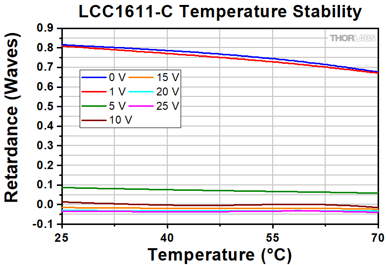
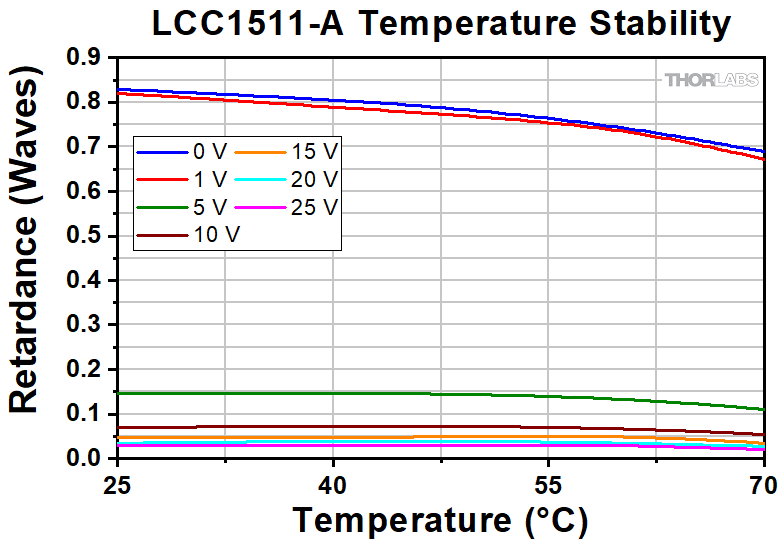
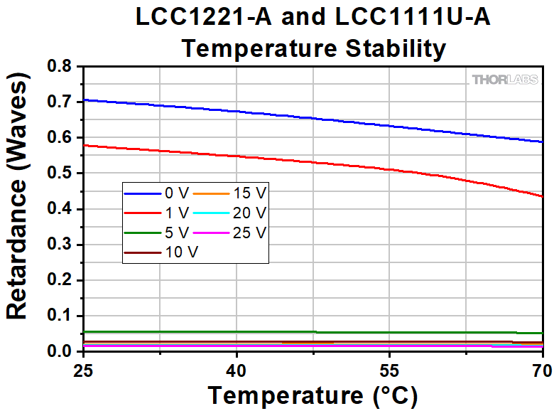
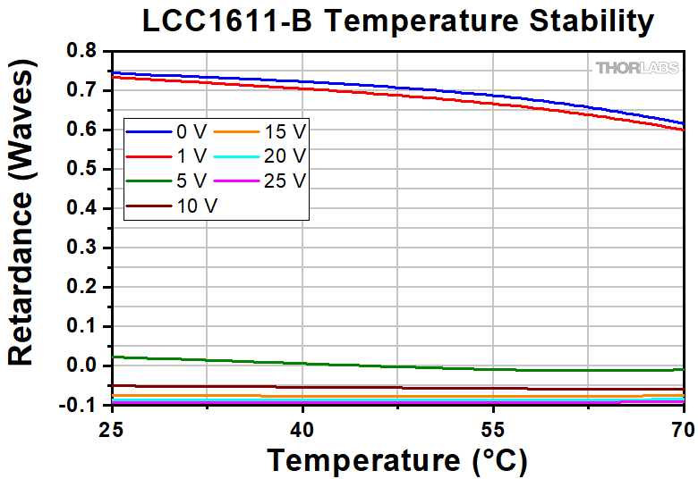
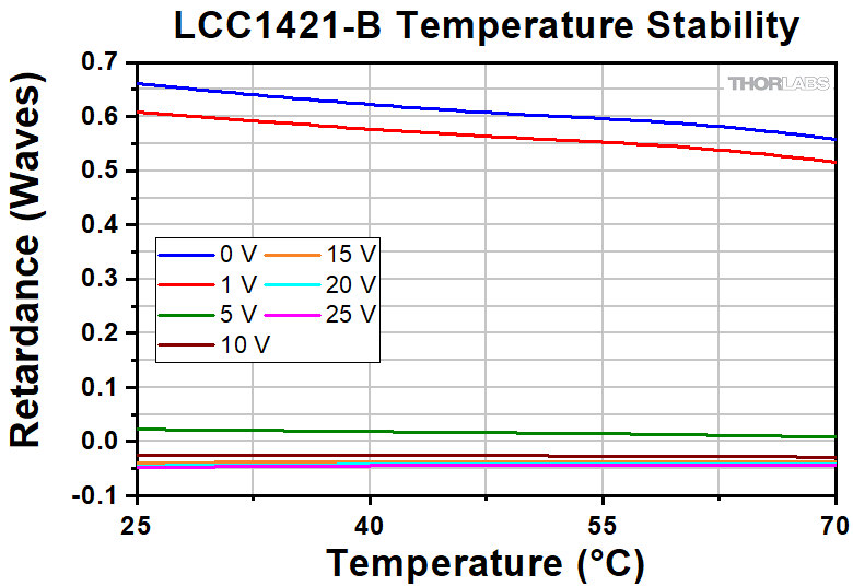
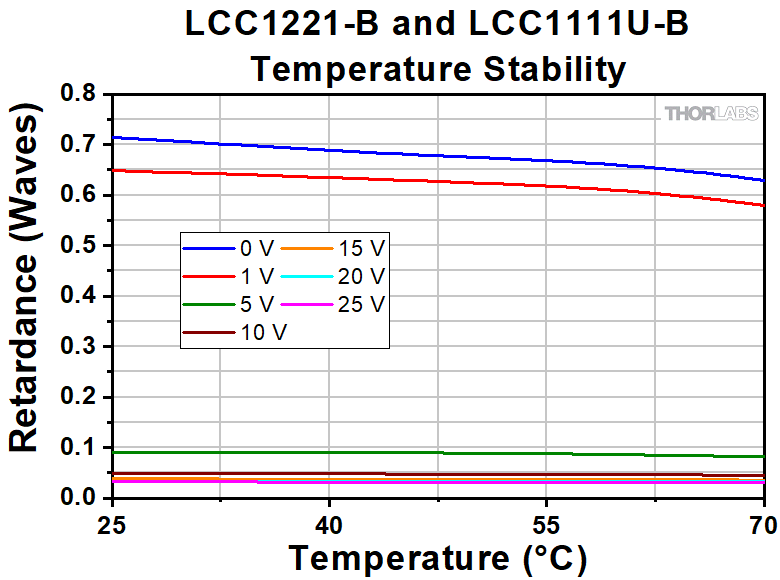
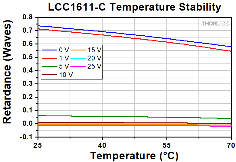
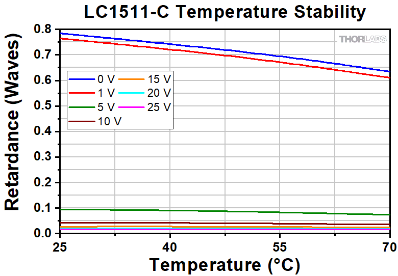
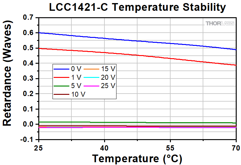
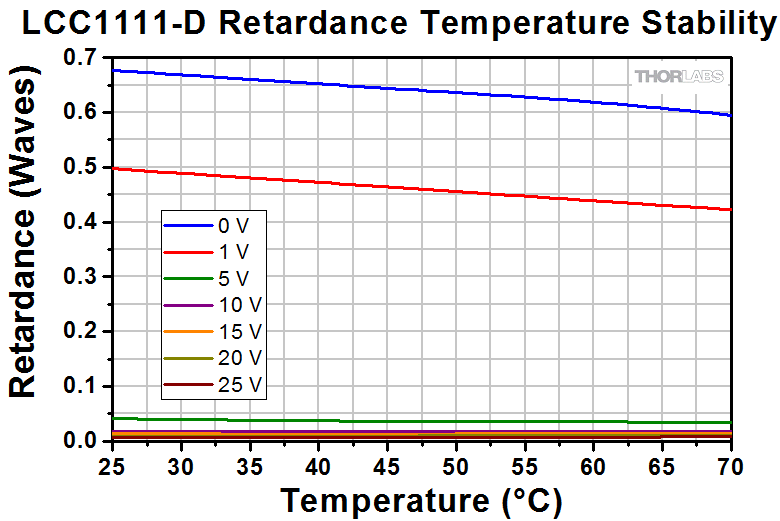
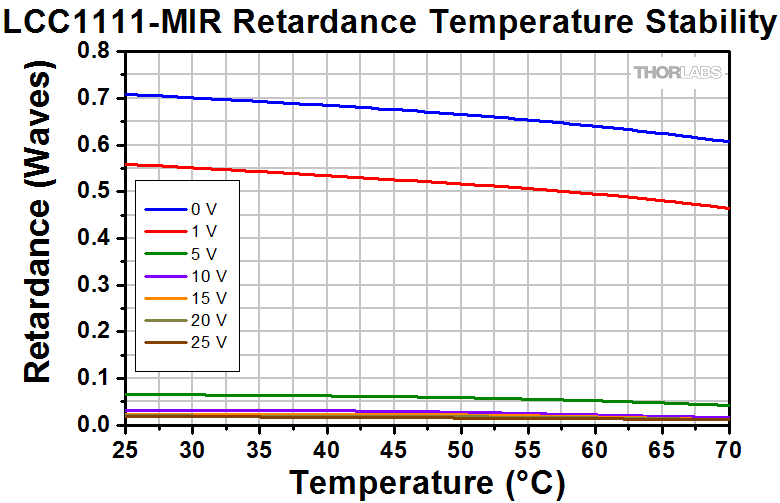
Temperature Stability
Our liquid crystal retarders have a retardance that slightly decreases with increasing temperature. The graphs in the table above compare the retardance at set drive voltages versus temperature. For temperature unregulated environments, Thorlabs' temperature controlled half-wave LCRs are suggested.
LCC1611 and LCC1511 Fast Switching Ø10 mm Clear Aperture LCVR DataClick Here to Download Temperature Stability Data
LCC1111-D and LCC1111-MIR Ø10 mm Clear Aperture LCVR Data
Click Here to Download Temperature Stability Data
LCC1421, LCC1221, and LCC1111U Ø10 mm Clear Aperture LCVR Data
Click Here to Download Temperature Stability Data
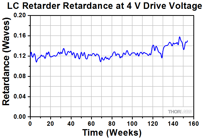
Click to Enlarge
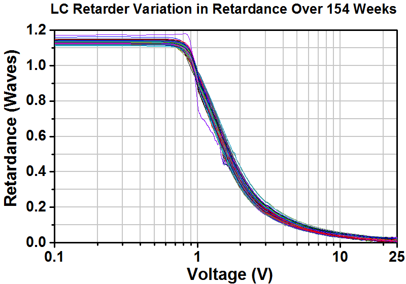
Graph shows variation in retardance over a period of 154 weeks.
Long-Term Stability
Our liquid crystal retarders exhibit consistent performance over time. The graph to the right shows the retardance vs. voltage for one previous-generation LCC1112-A three-quarter wave retarder, driven by our LCC25 liquid crystal controller over 154 weeks. The retardance was tested once per week and varied only slightly over the testing period. For the complete set of data from testing each week, please click below to download the full data file.
The graph below to the left shows that the retardance varies only slightly at a constant voltage, while the graph below to the right shows that the voltage varies only slightly at a constant retardance. Similar consistency in performance can also be expected for our other models of retarders. To maximize the long-term stability of our retarders, we recommend always using our LCC25 or KLC101 controllers. They are designed to reduce the DC voltage offset, thus minimizing charge buildup and maximizing stability.

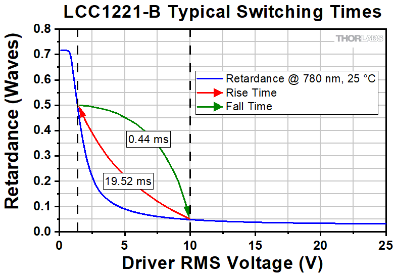
LC Retarders Switching Time
Liquid crystal retarders feature a short switching time compared to mechanical variable wave plates due to the lack of moving parts. The switching time of a liquid crystal retarder depends on several variables, some of which are controlled in the manufacturing process, and some by the user.
In general, liquid crystal retarders will always switch faster at a higher driving voltage than at a lower driving voltage. Also, the fall time (from low voltage to high voltage) is faster than rise time (from high voltage to low voltage) when the LC retarder is switched between two voltages. The graph to the right depicts an example of switching between 1.26 V and 10 V. If faster switching times are desired, we recommend using the retarder together with a fixed wave plate so that the retarder can be used at a higher voltage. Do not exceed the maximum voltage indicated in the Specs tab.
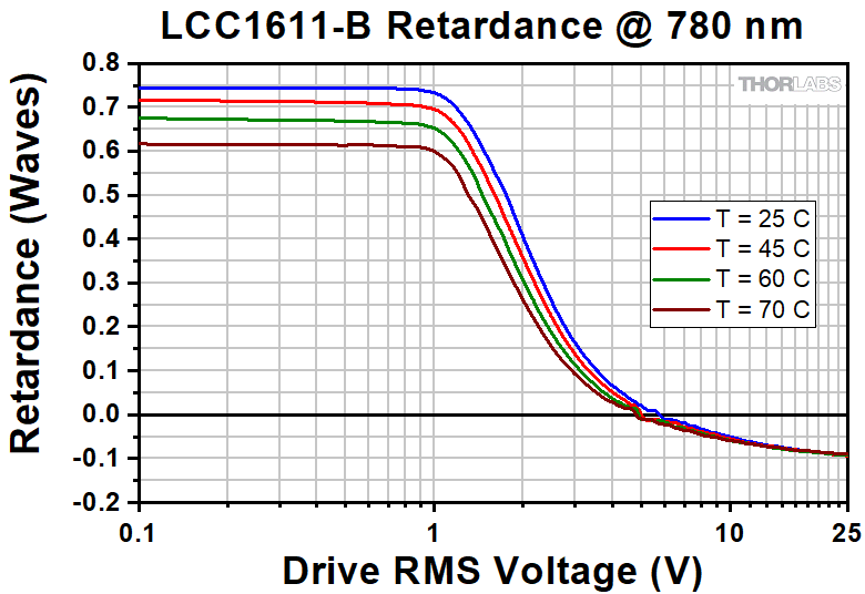
In addition, the material's viscosity and hence the switching time also depends on temperature of the LC material. As can be seen below, the switching time can increase by as much as two times by heating the LC retarder. Our standard LC retarders are designed to work at temperatures up to 45 °C, where they can still maintain the specified retardation. If faster switching times are required, the retarders can work at temperatures up to 70 °C, but the maximum retardation value may be lower. The specified half-wave retardation of λ/2 may not be achieved at temperatures of 70 °C or higher. Please see the switching time tables below for more information.
The switching time is also related to the thickness of the LC retarder, the rotational viscosity of the LC material, and the dielectric anisotropy of the LC material. However, since each of those variables affects other operating parameters as well, our LC retarders are designed to optimize overall performance, with a special emphasis on switching time. We also offer custom and OEM LC retarders optimized for other parameters, as well as faster liquid crystal retarders. See the Custom Capabilities tab above, or contact Tech Sales for details.
Sample Switching Times at Various Temperatures
Switching times were tested by measuring the rise time from V1 to V2 and the fall time from V2 to V1 with the liquid crystal retarder being held at the specified temperature. V1 is fixed at 10 V for all the tests, and V2 is the voltage at which the retardation is the maximum specified value for the retarder (λ/2). Please note that switching times at lower voltages (for instance, if V1 = 5 V) are longer than the switching times specified below.
Compensated Retarders
| LCC1611-A (AR Coating: 350 - 700 nm) |
||||
|---|---|---|---|---|
| Temperature | V1 | V2 | Rise Time | Fall Time |
| 25 °C | 10 | 2.00 | 3.34 ms | 0.14 ms |
| 45 °C | 10 | 1.80 | 2.44 ms | 0.10 ms |
| 60 °C | 10 | 1.70 | 1.82 ms | 0.09 ms |
| 70 °C | 10 | 1.50 | 1.33 ms | 0.07 ms |
| LCC1611-B (AR Coating: 650 - 1050 nm) |
||||
|---|---|---|---|---|
| Temperature | V1 | V2 | Rise Time | Fall Time |
| 25 °C | 10 | 1.75 | 4.01 ms | 0.27 ms |
| 45 °C | 10 | 1.60 | 3.14 ms | 0.21 ms |
| 60 °C | 10 | 1.45 | 2.55 ms | 0.16 ms |
| 70 °C | 10 | 1.30 | 2.31 ms | 0.15 ms |
| LCC1611-C (AR Coating: 1050 - 1700 nm) |
||||
|---|---|---|---|---|
| Temperature | V1 | V2 | Rise Time | Fall Time |
| 25 °C | 10 | 1.55 | 22.34 ms | 0.55 ms |
| 45 °C | 10 | 1.40 | 16.32 ms | 0.41 ms |
| 60 °C | 10 | 1.25 | 14.08 ms | 0.35 ms |
| 70 °C | 10 | 1.15 | 13.77 ms | 0.31 ms |
| LCC1421-Aa (AR Coating: 350 - 700 nm) |
||||
|---|---|---|---|---|
| Temperature | V1 | V2 | Rise Time | Fall Time |
| 22 °C | 10 | 1.18 | 15.8 ms | 260 µs |
| 45 °C | 10 | 1.02 | 8.56 ms | 176 µs |
| 60 °C | 10 | 0.9 | 7.39 ms | 122 µs |
| 70 °C | 10 | 0.8 | 6.42 ms | 106 µs |
| LCC1421-Ba (AR Coating: 650 - 1050 nm) |
||||
|---|---|---|---|---|
| Temperature | V1 | V2 | Rise Time | Fall Time |
| 22 °C | 10 | 1.26 | 34 ms | 360 µs |
| 45 °C | 10 | 1.16 | 19.6 ms | 243 µs |
| 60 °C | 10 | 1.10 | 15.1 ms | 123 µs |
| 70 °C | 10 | 1.02 | 12.6 ms | 101 µs |
| LCC1421-Ca (AR Coating: 1050 - 1700 nm) |
||||
|---|---|---|---|---|
| Temperature | V1 | V2 | Rise Time | Fall Time |
| 25.6 °C | 10 | 1.00 | 152 ms | 510 µs |
| 45 °C | 10 | 0.80 | 79.1 ms | 326 µs |
| 60 °C | 10 | 0.70 | 59.1 ms | 195 µs |
| 70 °C | 10 | 0.50b | 56.1 ms | 189 µs |
Uncompensated Retarders
| LCC1511-A (AR Coating: 350 - 700 nm) |
||||
|---|---|---|---|---|
| Temperature | V1 | V2 | Rise Time | Fall Time |
| 25 °C | 10 | 1.90 | 2.72 ms | 0.16 ms |
| 45 °C | 10 | 1.85 | 2.01 ms | 0.11 ms |
| 60 °C | 10 | 1.70 | 1.53 ms | 0.09 ms |
| 70 °C | 10 | 1.60 | 1.25 ms | 0.07 ms |
| LCC1511-B (AR Coating: 650 - 1050 nm) |
||||
|---|---|---|---|---|
| Temperature | V1 | V2 | Rise Time | Fall Time |
| 25 °C | 10 | 2.05 | 3.41 ms | 0.24 ms |
| 45 °C | 10 | 1.90 | 2.64 ms | 0.19 ms |
| 60 °C | 10 | 1.70 | 1.98 ms | 0.15 ms |
| 70 °C | 10 | 1.55 | 1.89 ms | 0.11 ms |
| LCC1511-C (AR Coating: 1050 - 1700 nm) |
||||
|---|---|---|---|---|
| Temperature | V1 | V2 | Rise Time | Fall Time |
| 25 °C | 10 | 1.65 | 21.29 ms | 0.50 ms |
| 45 °C | 10 | 1.55 | 14.8 ms | 0.41 ms |
| 60 °C | 10 | 1.40 | 12.67 ms | 0.30 ms |
| 70 °C | 10 | 1.30 | 10.8 ms | 0.23 ms |
| LCC1111U-A, LCC1221-Aa (AR Coating: 350 - 700 nm) |
||||
|---|---|---|---|---|
| Temperature | V1 | V2 | Rise Time | Fall Time |
| 22 °C | 10 | 1.14 | 10.2 ms | 310 µs |
| 45 °C | 10 | 1.08 | 5.85 ms | 211 µs |
| 60 °C | 10 | 1.00 | 5.05 ms | 146 µs |
| 70 °C | 10 | 0.90 | 4.55 ms | 126 µs |
| LCC1111U-B, LCC1221-Ba (AR Coating: 650 - 1050 nm) |
||||
|---|---|---|---|---|
| Temperature | V1 | V2 | Rise Time | Fall Time |
| 25 °C | 10 | 1.38 | 19.52 ms | 0.44 ms |
| 45 °C | 10 | 1.36 | 10.87 ms | 0.20 ms |
| 60 °C | 10 | 1.32 | 8.54 ms | 0.12 ms |
| 70 °C | 10 | 1.24 | 7.78 ms | 0.10 ms |
| LCC1221-Ca (AR Coating: 1050 - 1700 nm) |
||||
|---|---|---|---|---|
| Temperature | V1 | V2 | Rise Time | Fall Time |
| 25.6 °C | 10 | 1.00 | 95.8 ms | 1.18 ms |
| 45 °C | 10 | 0.90 | 66.4 ms | 1.16 ms |
| 60 °C | 10 | 0.90 | 49.7 ms | 692 µs |
| 70 °C | 10 | 0.10b | 47.2 ms | 671 µs |
| LCC1111-D (AR Coating: 1650 - 3000 nm) |
||||
|---|---|---|---|---|
| Temperature | V1 | V2 | Rise Time | Fall Time |
| 25.6 °C | 10 | 0.99 | 192 ms | 1.0 ms |
| 45 °C | 10 | 0.92 | 80 ms | 0.8 ms |
| 60 °C | 10 | 0.88 | 50 ms | 0.5 ms |
| 70 °C | 10 | 0.86 | 44 ms | 0.2 ms |
| LCC1111-MIR (AR Coating: 3600 - 5600 nm) |
||||
|---|---|---|---|---|
| Temperature | V1 | V2 | Rise Time | Fall Time |
| 25.6 °C | 10 | 1.14 | 372 ms | 14 ms |
| 45 °C | 10 | 1.05 | 204 ms | 6.9 ms |
| 60 °C | 10 | 0.99 | 180 ms | 3.6 ms |
| 70 °C | 10 | 0.94 | 150 ms | 1.6 ms |
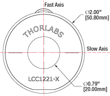
Drawing indicates the slow and fast axes
Alignment
The slow (extraordinary) axis of the liquid crystal retarder corresponds to the orientation of the long axis of the liquid crystal molecules when no voltage is being applied. Applying a voltage will cause the orientation direction of the liquid crystal molecules to rotate out of the plane of the drawing to the right, changing the retardation. Thorlabs LC retarders are nematic liquid crystal devices, which must be driven with an AC voltage in order to prevent the accumulation of ions and free charges, which degrades performance and can cause the device to burn out.
In order to precisely align the axis of the liquid crystal cell, mount the retarder in an appropriate rotation mount (e.g. the RSP1(/M) or CRM1P(/M) for our Ø10 mm clear aperture retarders and the RSP2(/M) or LCRM2A(/M) for our Ø20 mm clear aperture retarders). Then set up a detector or power meter to monitor the transmission of a beam through a pair of crossed linear polarizers. Next place the LC retarder between two crossed polarizers with the slow axis aligned with the transmission axis of the first polarizer. Then slowly rotate it until the transmitted intensity is minimized. In this configuration, the LC retarder is ready for phase modulation applications.
To operate as a light intensity modulator or shutter, again find the minimum transmitted intensity as prescribed above. Once the minimum is found, rotate the retarder by ±45°. This will maximize the transmitted intensity through the crossed polarizers for most LC retarders (e.g., zero-order quarter- or half-wave plates). However, this rule of thumb does not rigidly hold for multi-wave phase retarders using broadband sources due to the wavelength dependency of the retardation.
Applications
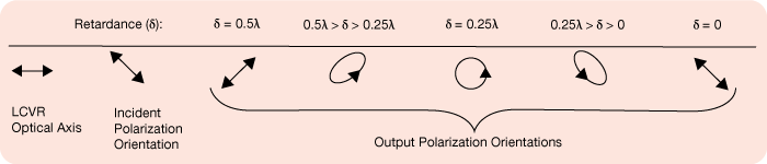
Polarization Control with a Liquid Crystal Variable Retarder
The LCVR can be effectively used as a variable zero-order wave plate over a broad spectrum of wavelengths. The optical axis of the LCVR is defined as the major axis of the liquid crystal molecules when no voltage is being applied to the cell, which are all aligned due to the LC alignment layer. When using the LCVR to control the polarization of a beam, the linearly polarized input beam should be aligned so that its polarization axis is oriented at an angle of 45° with respect to the optical axis of the LCVR in order to maximize the dynamic range of the optic. The schematic below shows how the output state of polarization will change as retardance is decreased (RMS voltage increased).
Pure Phase Retarder with Liquid Crystal Variable Retarder
In order to only effect the phase of the incident beam, the linearly polarized input beam must have its polarization axis aligned with the optical axis of the liquid crystal retarder. As VRMS is increased, the phase offset in the beam is decreased. Pure phase retarders are often used in interferometers to alter the optical path length of one arm of the interferometer with respect to the other. With an LCVR, this can be done actively.
| Damage Threshold Specifications | ||
|---|---|---|
| Item # Suffix |
Laser Type | Damage Threshold |
| -A | Pulsed (ns) | 1.0 J/cm2 (532 nm, 10 Hz, 8 ns, Ø200 µm) |
| Pulsed (fs) | 0.01 J/cm2 (532 nm, 100 Hz, 76 fs, Ø162 µm) | |
| -B | Pulsed (ns) | 1.7 J/cm2 (810 nm, 10 Hz, 7.6 ns, Ø234 µm) |
| Pulsed (fs) | 0.01 J/cm2 (800 nm, 100 Hz, 36.4 fs, Ø189 µm) | |
| -C | Pulsed (ns) | 1.2 J/cm2 (1542 nm, 10 Hz, 10 ns, Ø458 µm) |
| Pulsed (fs) | 0.08 J/cm2 (1550 nm, 100 Hz, 70 fs, Ø145 µm) | |
| -D | Pulsed (ns) | 0.041 J/cm2 (2000 nm, 10 Hz, 6.5 ns, Ø292 µm) |
| Pulsed (fs) | 0.025 J/cm2 (2000 nm, 100 Hz, 100 fs, Ø220 µm) | |
Damage Threshold Data for Thorlabs' Liquid Crystal Variable Retarders
The specifications to the right are measured data for Thorlabs' Liquid Crystal Variable Retarders.
Laser Induced Damage Threshold Tutorial
The following is a general overview of how laser induced damage thresholds are measured and how the values may be utilized in determining the appropriateness of an optic for a given application. When choosing optics, it is important to understand the Laser Induced Damage Threshold (LIDT) of the optics being used. The LIDT for an optic greatly depends on the type of laser you are using. Continuous wave (CW) lasers typically cause damage from thermal effects (absorption either in the coating or in the substrate). Pulsed lasers, on the other hand, often strip electrons from the lattice structure of an optic before causing thermal damage. Note that the guideline presented here assumes room temperature operation and optics in new condition (i.e., within scratch-dig spec, surface free of contamination, etc.). Because dust or other particles on the surface of an optic can cause damage at lower thresholds, we recommend keeping surfaces clean and free of debris. For more information on cleaning optics, please see our Optics Cleaning tutorial.
Testing Method
Thorlabs' LIDT testing is done in compliance with ISO/DIS 11254 and ISO 21254 specifications.
First, a low-power/energy beam is directed to the optic under test. The optic is exposed in 10 locations to this laser beam for 30 seconds (CW) or for a number of pulses (pulse repetition frequency specified). After exposure, the optic is examined by a microscope (~100X magnification) for any visible damage. The number of locations that are damaged at a particular power/energy level is recorded. Next, the power/energy is either increased or decreased and the optic is exposed at 10 new locations. This process is repeated until damage is observed. The damage threshold is then assigned to be the highest power/energy that the optic can withstand without causing damage. A histogram such as that below represents the testing of one BB1-E02 mirror.
The photograph above is a protected aluminum-coated mirror after LIDT testing. In this particular test, it handled 0.43 J/cm2 (1064 nm, 10 ns pulse, 10 Hz, Ø1.000 mm) before damage.
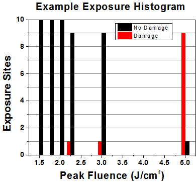
| Example Test Data | |||
|---|---|---|---|
| Fluence | # of Tested Locations | Locations with Damage | Locations Without Damage |
| 1.50 J/cm2 | 10 | 0 | 10 |
| 1.75 J/cm2 | 10 | 0 | 10 |
| 2.00 J/cm2 | 10 | 0 | 10 |
| 2.25 J/cm2 | 10 | 1 | 9 |
| 3.00 J/cm2 | 10 | 1 | 9 |
| 5.00 J/cm2 | 10 | 9 | 1 |
According to the test, the damage threshold of the mirror was 2.00 J/cm2 (532 nm, 10 ns pulse, 10 Hz, Ø0.803 mm). Please keep in mind that these tests are performed on clean optics, as dirt and contamination can significantly lower the damage threshold of a component. While the test results are only representative of one coating run, Thorlabs specifies damage threshold values that account for coating variances.
Continuous Wave and Long-Pulse Lasers
When an optic is damaged by a continuous wave (CW) laser, it is usually due to the melting of the surface as a result of absorbing the laser's energy or damage to the optical coating (antireflection) [1]. Pulsed lasers with pulse lengths longer than 1 µs can be treated as CW lasers for LIDT discussions.
When pulse lengths are between 1 ns and 1 µs, laser-induced damage can occur either because of absorption or a dielectric breakdown (therefore, a user must check both CW and pulsed LIDT). Absorption is either due to an intrinsic property of the optic or due to surface irregularities; thus LIDT values are only valid for optics meeting or exceeding the surface quality specifications given by a manufacturer. While many optics can handle high power CW lasers, cemented (e.g., achromatic doublets) or highly absorptive (e.g., ND filters) optics tend to have lower CW damage thresholds. These lower thresholds are due to absorption or scattering in the cement or metal coating.
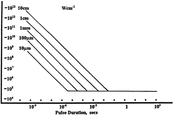
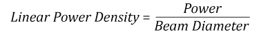
LIDT in linear power density vs. pulse length and spot size. For long pulses to CW, linear power density becomes a constant with spot size. This graph was obtained from [1].
Pulsed lasers with high pulse repetition frequencies (PRF) may behave similarly to CW beams. Unfortunately, this is highly dependent on factors such as absorption and thermal diffusivity, so there is no reliable method for determining when a high PRF laser will damage an optic due to thermal effects. For beams with a high PRF both the average and peak powers must be compared to the equivalent CW power. Additionally, for highly transparent materials, there is little to no drop in the LIDT with increasing PRF.
In order to use the specified CW damage threshold of an optic, it is necessary to know the following:
- Wavelength of your laser
- Beam diameter of your beam (1/e2)
- Approximate intensity profile of your beam (e.g., Gaussian)
- Linear power density of your beam (total power divided by 1/e2 beam diameter)
Thorlabs expresses LIDT for CW lasers as a linear power density measured in W/cm. In this regime, the LIDT given as a linear power density can be applied to any beam diameter; one does not need to compute an adjusted LIDT to adjust for changes in spot size, as demonstrated by the graph to the right. Average linear power density can be calculated using the equation below.
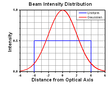
The calculation above assumes a uniform beam intensity profile. You must now consider hotspots in the beam or other non-uniform intensity profiles and roughly calculate a maximum power density. For reference, a Gaussian beam typically has a maximum power density that is twice that of the uniform beam (see lower right).
Now compare the maximum power density to that which is specified as the LIDT for the optic. If the optic was tested at a wavelength other than your operating wavelength, the damage threshold must be scaled appropriately. A good rule of thumb is that the damage threshold has a linear relationship with wavelength such that as you move to shorter wavelengths, the damage threshold decreases (i.e., a LIDT of 10 W/cm at 1310 nm scales to 5 W/cm at 655 nm):
While this rule of thumb provides a general trend, it is not a quantitative analysis of LIDT vs wavelength. In CW applications, for instance, damage scales more strongly with absorption in the coating and substrate, which does not necessarily scale well with wavelength. While the above procedure provides a good rule of thumb for LIDT values, please contact Tech Support if your wavelength is different from the specified LIDT wavelength. If your power density is less than the adjusted LIDT of the optic, then the optic should work for your application.
Please note that we have a buffer built in between the specified damage thresholds online and the tests which we have done, which accommodates variation between batches. Upon request, we can provide individual test information and a testing certificate. The damage analysis will be carried out on a similar optic (customer's optic will not be damaged). Testing may result in additional costs or lead times. Contact Tech Support for more information.
Pulsed Lasers
As previously stated, pulsed lasers typically induce a different type of damage to the optic than CW lasers. Pulsed lasers often do not heat the optic enough to damage it; instead, pulsed lasers produce strong electric fields capable of inducing dielectric breakdown in the material. Unfortunately, it can be very difficult to compare the LIDT specification of an optic to your laser. There are multiple regimes in which a pulsed laser can damage an optic and this is based on the laser's pulse length. The highlighted columns in the table below outline the relevant pulse lengths for our specified LIDT values.
Pulses shorter than 10-9 s cannot be compared to our specified LIDT values with much reliability. In this ultra-short-pulse regime various mechanics, such as multiphoton-avalanche ionization, take over as the predominate damage mechanism [2]. In contrast, pulses between 10-7 s and 10-4 s may cause damage to an optic either because of dielectric breakdown or thermal effects. This means that both CW and pulsed damage thresholds must be compared to the laser beam to determine whether the optic is suitable for your application.
| Pulse Duration | t < 10-9 s | 10-9 < t < 10-7 s | 10-7 < t < 10-4 s | t > 10-4 s |
|---|---|---|---|---|
| Damage Mechanism | Avalanche Ionization | Dielectric Breakdown | Dielectric Breakdown or Thermal | Thermal |
| Relevant Damage Specification | No Comparison (See Above) | Pulsed | Pulsed and CW | CW |
When comparing an LIDT specified for a pulsed laser to your laser, it is essential to know the following:
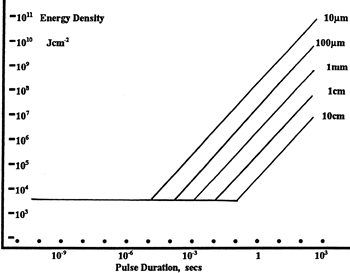
LIDT in energy density vs. pulse length and spot size. For short pulses, energy density becomes a constant with spot size. This graph was obtained from [1].
- Wavelength of your laser
- Energy density of your beam (total energy divided by 1/e2 area)
- Pulse length of your laser
- Pulse repetition frequency (prf) of your laser
- Beam diameter of your laser (1/e2 )
- Approximate intensity profile of your beam (e.g., Gaussian)
The energy density of your beam should be calculated in terms of J/cm2. The graph to the right shows why expressing the LIDT as an energy density provides the best metric for short pulse sources. In this regime, the LIDT given as an energy density can be applied to any beam diameter; one does not need to compute an adjusted LIDT to adjust for changes in spot size. This calculation assumes a uniform beam intensity profile. You must now adjust this energy density to account for hotspots or other nonuniform intensity profiles and roughly calculate a maximum energy density. For reference a Gaussian beam typically has a maximum energy density that is twice that of the 1/e2 beam.
Now compare the maximum energy density to that which is specified as the LIDT for the optic. If the optic was tested at a wavelength other than your operating wavelength, the damage threshold must be scaled appropriately [3]. A good rule of thumb is that the damage threshold has an inverse square root relationship with wavelength such that as you move to shorter wavelengths, the damage threshold decreases (i.e., a LIDT of 1 J/cm2 at 1064 nm scales to 0.7 J/cm2 at 532 nm):
You now have a wavelength-adjusted energy density, which you will use in the following step.
Beam diameter is also important to know when comparing damage thresholds. While the LIDT, when expressed in units of J/cm², scales independently of spot size; large beam sizes are more likely to illuminate a larger number of defects which can lead to greater variances in the LIDT [4]. For data presented here, a <1 mm beam size was used to measure the LIDT. For beams sizes greater than 5 mm, the LIDT (J/cm2) will not scale independently of beam diameter due to the larger size beam exposing more defects.
The pulse length must now be compensated for. The longer the pulse duration, the more energy the optic can handle. For pulse widths between 1 - 100 ns, an approximation is as follows:
Use this formula to calculate the Adjusted LIDT for an optic based on your pulse length. If your maximum energy density is less than this adjusted LIDT maximum energy density, then the optic should be suitable for your application. Keep in mind that this calculation is only used for pulses between 10-9 s and 10-7 s. For pulses between 10-7 s and 10-4 s, the CW LIDT must also be checked before deeming the optic appropriate for your application.
Please note that we have a buffer built in between the specified damage thresholds online and the tests which we have done, which accommodates variation between batches. Upon request, we can provide individual test information and a testing certificate. Contact Tech Support for more information.
[1] R. M. Wood, Optics and Laser Tech. 29, 517 (1998).
[2] Roger M. Wood, Laser-Induced Damage of Optical Materials (Institute of Physics Publishing, Philadelphia, PA, 2003).
[3] C. W. Carr et al., Phys. Rev. Lett. 91, 127402 (2003).
[4] N. Bloembergen, Appl. Opt. 12, 661 (1973).

In order to illustrate the process of determining whether a given laser system will damage an optic, a number of example calculations of laser induced damage threshold are given below. For assistance with performing similar calculations, we provide a spreadsheet calculator that can be downloaded by clicking the button to the right. To use the calculator, enter the specified LIDT value of the optic under consideration and the relevant parameters of your laser system in the green boxes. The spreadsheet will then calculate a linear power density for CW and pulsed systems, as well as an energy density value for pulsed systems. These values are used to calculate adjusted, scaled LIDT values for the optics based on accepted scaling laws. This calculator assumes a Gaussian beam profile, so a correction factor must be introduced for other beam shapes (uniform, etc.). The LIDT scaling laws are determined from empirical relationships; their accuracy is not guaranteed. Remember that absorption by optics or coatings can significantly reduce LIDT in some spectral regions. These LIDT values are not valid for ultrashort pulses less than one nanosecond in duration.
A Gaussian beam profile has about twice the maximum intensity of a uniform beam profile.
CW Laser Example
Suppose that a CW laser system at 1319 nm produces a 0.5 W Gaussian beam that has a 1/e2 diameter of 10 mm. A naive calculation of the average linear power density of this beam would yield a value of 0.5 W/cm, given by the total power divided by the beam diameter:
However, the maximum power density of a Gaussian beam is about twice the maximum power density of a uniform beam, as shown in the graph to the right. Therefore, a more accurate determination of the maximum linear power density of the system is 1 W/cm.
An AC127-030-C achromatic doublet lens has a specified CW LIDT of 350 W/cm, as tested at 1550 nm. CW damage threshold values typically scale directly with the wavelength of the laser source, so this yields an adjusted LIDT value:
The adjusted LIDT value of 350 W/cm x (1319 nm / 1550 nm) = 298 W/cm is significantly higher than the calculated maximum linear power density of the laser system, so it would be safe to use this doublet lens for this application.
Pulsed Nanosecond Laser Example: Scaling for Different Pulse Durations
Suppose that a pulsed Nd:YAG laser system is frequency tripled to produce a 10 Hz output, consisting of 2 ns output pulses at 355 nm, each with 1 J of energy, in a Gaussian beam with a 1.9 cm beam diameter (1/e2). The average energy density of each pulse is found by dividing the pulse energy by the beam area:
As described above, the maximum energy density of a Gaussian beam is about twice the average energy density. So, the maximum energy density of this beam is ~0.7 J/cm2.
The energy density of the beam can be compared to the LIDT values of 1 J/cm2 and 3.5 J/cm2 for a BB1-E01 broadband dielectric mirror and an NB1-K08 Nd:YAG laser line mirror, respectively. Both of these LIDT values, while measured at 355 nm, were determined with a 10 ns pulsed laser at 10 Hz. Therefore, an adjustment must be applied for the shorter pulse duration of the system under consideration. As described on the previous tab, LIDT values in the nanosecond pulse regime scale with the square root of the laser pulse duration:
This adjustment factor results in LIDT values of 0.45 J/cm2 for the BB1-E01 broadband mirror and 1.6 J/cm2 for the Nd:YAG laser line mirror, which are to be compared with the 0.7 J/cm2 maximum energy density of the beam. While the broadband mirror would likely be damaged by the laser, the more specialized laser line mirror is appropriate for use with this system.
Pulsed Nanosecond Laser Example: Scaling for Different Wavelengths
Suppose that a pulsed laser system emits 10 ns pulses at 2.5 Hz, each with 100 mJ of energy at 1064 nm in a 16 mm diameter beam (1/e2) that must be attenuated with a neutral density filter. For a Gaussian output, these specifications result in a maximum energy density of 0.1 J/cm2. The damage threshold of an NDUV10A Ø25 mm, OD 1.0, reflective neutral density filter is 0.05 J/cm2 for 10 ns pulses at 355 nm, while the damage threshold of the similar NE10A absorptive filter is 10 J/cm2 for 10 ns pulses at 532 nm. As described on the previous tab, the LIDT value of an optic scales with the square root of the wavelength in the nanosecond pulse regime:
This scaling gives adjusted LIDT values of 0.08 J/cm2 for the reflective filter and 14 J/cm2 for the absorptive filter. In this case, the absorptive filter is the best choice in order to avoid optical damage.
Pulsed Microsecond Laser Example
Consider a laser system that produces 1 µs pulses, each containing 150 µJ of energy at a repetition rate of 50 kHz, resulting in a relatively high duty cycle of 5%. This system falls somewhere between the regimes of CW and pulsed laser induced damage, and could potentially damage an optic by mechanisms associated with either regime. As a result, both CW and pulsed LIDT values must be compared to the properties of the laser system to ensure safe operation.
If this relatively long-pulse laser emits a Gaussian 12.7 mm diameter beam (1/e2) at 980 nm, then the resulting output has a linear power density of 5.9 W/cm and an energy density of 1.2 x 10⁻⁴ J/cm2 per pulse. This can be compared to the LIDT values for a WPQ10E-980 polymer zero-order quarter-wave plate, which are 5 W/cm for CW radiation at 810 nm and 5 J/cm2 for a 10 ns pulse at 810 nm. As before, the CW LIDT of the optic scales linearly with the laser wavelength, resulting in an adjusted CW value of 6 W/cm at 980 nm. On the other hand, the pulsed LIDT scales with the square root of the laser wavelength and the square root of the pulse duration, resulting in an adjusted value of 55 J/cm2 for a 1 µs pulse at 980 nm. The pulsed LIDT of the optic is significantly greater than the energy density of the laser pulse, so individual pulses will not damage the wave plate. However, the large average linear power density of the laser system may cause thermal damage to the optic, much like a high-power CW beam.
Previous Generation Ø10 mm Half-Wave Liquid Crystal Retarders Offered As Specials
The following table lists the current and previous generation of Ø10 mm half-wave LC retarders. The previous generation of Ø10 mm retarders listed below are available upon request by contacting Tech Sales.
| Half-Wave Ø10 mm Compensated LC Retarders | ||||
|---|---|---|---|---|
| Wavelength Range | Current Generation | Previous Generation | ||
| Item # | Switching Time (Rise/Fall) | Item # | Switching Time (Rise/Fall) | |
| 350 - 700 nm | LCC1611-A | 3.34 ms / 0.14 ms @ 25 °C, 635 nm | LCC1411-A | 15.8 ms / 260 µs @ 22 °C, 635 nm |
| 650 - 1050 nm | LCC1611-B | 4.01 ms / 0.27 ms @ 25 °C, 780 nm | LCC1411-B | 34.0 ms / 360 µs @ 22 °C, 780 nm |
| 1050 - 1700 nm | LCC1611-C | 22.34 ms / 0.55 ms @ 25 °C, 1550 nm | LCC1411-C | 152 ms / 510 µs @ 25.6 °C, 1550 nm |
| Half-Wave Ø10 mm Uncompensated LC Retarders | ||||
|---|---|---|---|---|
| Wavelength Range | Current Generation | Previous Generation | ||
| Item # | Switching Time (Rise/Fall) | Item # | Switching Time (Rise/Fall) | |
| 350 - 700 nm | LCC1511-A | 2.72 ms / 0.16 ms @ 25 °C, 635 nm | LCC1111-A | 10.2 ms / 310 µs @ 22 °C, 635 nm |
| 650 - 1050 nm | LCC1511-B | 3.41 ms / 0.24 ms @ 25 °C, 780 nm | LCC1111-B | 31.3 ms / 704 µs @ 25.6 °C, 780 nm |
| 1050 - 1700 nm | LCC1511-C | 21.29 ms / 0.50 ms @ 25 °C, 1550 nm | LCC1111-C | 95.8 ms / 1.81 ms @ 25.6 °C, 1550 nm |
Thorlabs' Custom Liquid Crystal Capabilities
Thorlabs offers a large variety of liquid crystal retarders from stock, including 1/2-, 3/4-, and full-wave models with a Ø10 mm or Ø20 mm clear aperture as well as 1/2-wave temperature-controlled models. However, we also offer OEM and custom retarders. The retardance range, coating, rubbing angle, temperature stabilization, and size can be customized to meet many unique optical designs. We also offer other custom liquid crystal devices, such as empty LC cells, polarization rotators, and noise eaters. For more information about ordering a custom liquid crystal device, please contact Thorlabs' technical support.
Our engineers work directly with our customers to discuss the specifications and other design aspects of a custom liquid crystal retarder. They will analyze both the design and feasibility to ensure the custom products are manufactured to high-quality standards and in a timely manner.
Polyimide (PI) Coating and Rubbing - Custom Alignment Angle
In their nematic phase, liquid crystal molecules naturally align to an average orientation, which together with their stretched shape, creates an optical anisotropy, or direction-dependent optical effect. The orientation of the LC molecules in an LC cell, in the absence of an applied voltage, is determined by the alignment layer, created by the polyimide (PI) coating and rubbing angle. Rubbing creates grooves, which the liquid crystal molecules will align to. Users can choose any initial orientation of LC molecules by specifying the rubbing angle.
Custom Cell Spacing
The wall spacing inside of the liquid crystal cell, which determines the thickness of LC material, can be customized during the manufacturing process. The retardance range of an LC cell is dependent on the LC material thickness:
![]()
Here, δ is the retardance in waves, d is the thickness of the LC material, λν is the wavelength of light, and Δn is the birefringence of the LC material used. Thus, for a given wavelength, the retardance is determined by the wall spacing inside the LC cell (i.e., the thickness of LC layer). We offer standard retardance ranges of λ/2 to 30 nm, 3λ/4 to 30 nm, and λ to 30 nm, but higher retardance ranges may also be ordered.
Custom Liquid Crystal Material
Customers can also provide their own liquid crystal material, and Thorlabs will use it to fill the liquid crystal cell. Since different liquid crystal materials have different birefringence values, varying the material enables a different retardance range.
Temperature Control/Switching Time
A temperature sensor can also be integrated into the LC variable retarder. Using a temperature controller, the temperature of the retarder can be actively stabilized to within ±0.1 °C. The viscosity of the liquid crystal material is lowered at higher temperatures, allowing the retarder to switch from one state to another due to the decreased viscosity. An active temperature control system can be used to heat the retarder, allowing it to operate at higher switching speeds.
Assembly / Housing
If desired, we can manufacture custom liquid crystal retarders without housings.
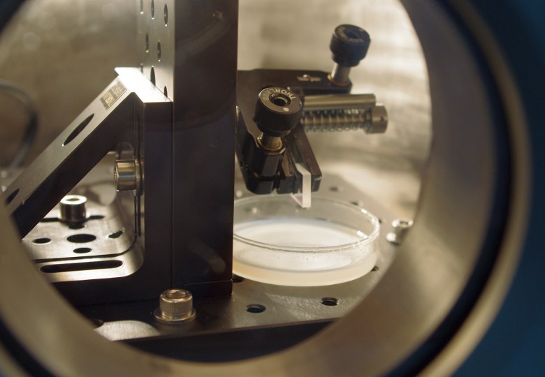
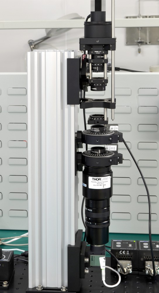
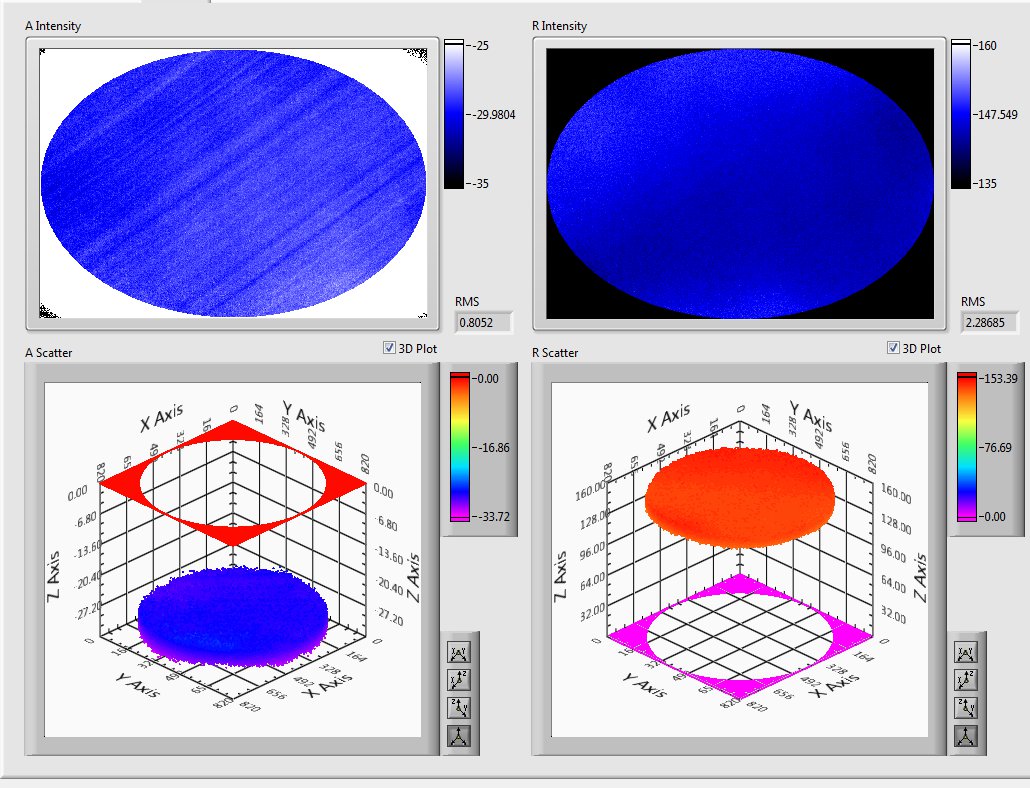
Testing
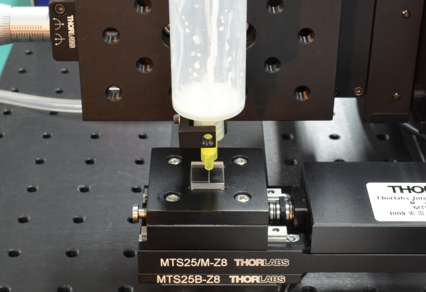
Each LC retarder is tested for birefringence, uniformity, and fast axis angle, using the measurement setup shown in the photo to the left. The equipment measures the 2-dimensional birefringence distribution using wave plates and a CCD camera. The image to the right shows a sample test result of a liquid crystal retarder, showing excellent uniformity.
For More Information
Contact Thorlabs' technical support for more information about our custom liquid crystal device options or to place an order.
| Custom Capability | Custom Specification |
|---|---|
| Patterned Retarder Size | Ø100 µm to Ø2" |
| Patterned Retarder Shape | Any |
| Microretarder Size | ≥Ø30 µm |
| Microretarder Shape | Round or Square |
| Retardance Range @ 632.8 nm | 50 to 550 nm |
| Substrate | N-BK7, UV Fused Silica, or Other Glass |
| Substrate Size | Ø5 mm to Ø2" |
| AR Coating | -A: 350 - 700 nm -B: 650 - 1050 nm -C: 1050 - 1700 nm |
Click to Enlarge
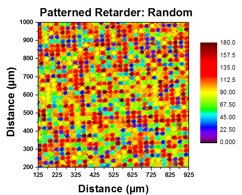
Figure 1: Patterned Retarder with Random Distribution
Features
- Build a Custom Microretarder
- Customize Size, Shape, and Substrate Material
- Retardance Range: 50 - 550 nm
- Fast Axis Resolution: <1º
- Retardance Fluctuations Under 30 nm
Applications
- 3D Displays
- Polarization Imaging
- Diffractive Optical Applications: Polarization Gratings, Polarimetry, and Beam Steering
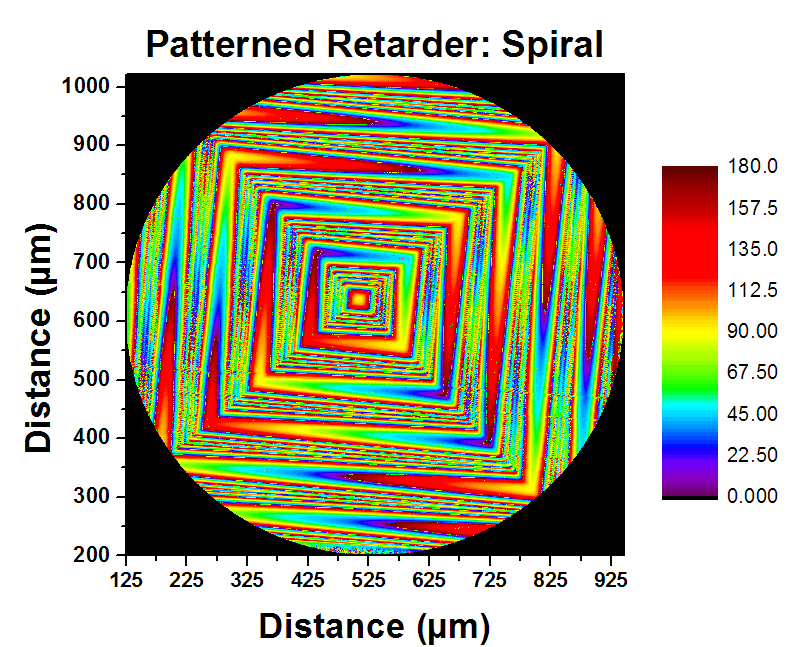
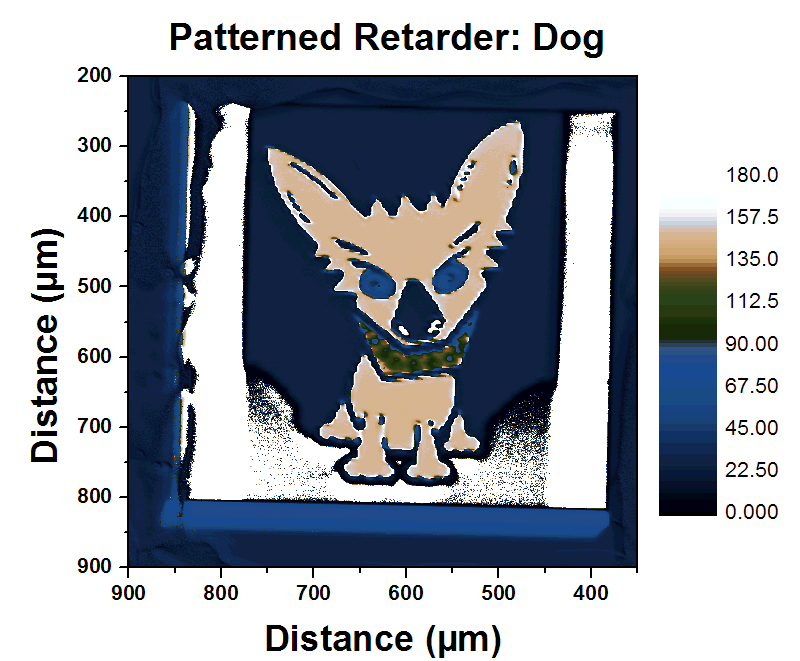
Thorlabs offers customizable patterned retarders, available in any pattern size from Ø100 µm to Ø2" and any substrate size from Ø5 mm to Ø2". These custom retarders are composed of an array of microretarders, each of which has a fast axis aligned to a different angle than its neighbor. The size and shape of the microretarders are also customizable. They can be as small as 30 µm and in shapes including circles and squares. This control over size and shape of the individual microretarders allows us to construct a large array of various patterned retarders to meet nearly any experimental or device need.
These patterned retarders are constructed from our liquid crystals and liquid crystal polymers. Using photo alignment technology, we can secure the fast axis of each microretarder to any angle within a resolution of <1°. Figures 1 - 3 show examples of our patterned retarders. The figures represent measured results of the patterned retarder captured on an imaging polarimeter and demonstrate that the fast axis orientation of any one individual microretarder can be controlled deterministically and separately from its neighbors.
The manufacturing process for our patterned retarders is controlled completely in house. It begins by preparing the substrate, which is typically N-BK7 or UV fused silica (although other glass substrates may be compatible as well). The substrate is then coated with a layer of photoalignment material and placed in our patterned retarder system where sections are exposed to linearly polarized light to set the fast axis of a microretarder. The area of the exposed sections depends on the desired size of the microretarder; the fast axis can be set between 0° and 180° with a resolution <1°. Once set, the liquid crystal cell is constructed by coating the device with a liquid crystal polymer and curing it with UV light.
Thorlabs' LCP depolarizers provide one example of these patterned retarders. In principle, a truly randomized pattern may be used as a depolarizer, since it scrambles the input polarization spatially. However, such a pattern will also introduce a large amount of diffraction. For our depolarizers, we designed a linearly ramping fast axis angle and retardance that can depolarize both broadband and monochromatic beams down to diameters of 0.5 mm without introducing additional diffraction. For more details, see the webpage for our LCP depolarizers.
By supplying Thorlabs with a drawing of the desired patterned retarder or an excel file of the fast axis distribution, we can construct almost any patterned retarder. For more information on creating a patterned retarder, please contact Tech Support.
Click to Enlarge
Figure 2: Patterned Retarder with a Spiral Distribution
Click to Enlarge
Figure 3: Patterned Retarder with a Pictoral Distribution
KLC101 Software
Version 1.0.0
GUI Interface for controlling the KLC101 Liquid Crystal Contoller via a PC. To download, click the button below.
LCC25 Software
Version 4.0.0
GUI Interface for controlling the LCC25 Liquid Crystal Controller via a PC. To download, click the button below.
| Posted Comments: | |
Yingliang Liu
(posted 2023-03-15 17:20:02.45) in our setup,we would like to rotate this liquid crystal half wave plate. we have fiound that the pointing direction of the laser has been changed after passing it. Is this normal? or there is a problem with the one we received from you.
By the way, have you considering this effect when you manufacturing this product? is there a way to get rid of the deviation the the beam direction after passing this wave plate when rotating it. For me, It seems that the front surface of this plate is not parallel withthe back surface. cdolbashian
(posted 2023-04-03 02:13:15.0) Thank you for contacting Thorlabs. Our half-wave liquid crystal variable retarders can actively control the phase delay or the polarization state of the light by applying a voltage to the liquid crystal cell. We don't need to rotate the retarder when using it, and the absence of moving parts provides quick switching times on the order of milliseconds. As for the beam deviation, we state it is less than 5 arcmin in the spec. We'll reach out to you via email to discuss your application. Jong-Min Yoon
(posted 2021-04-21 21:34:13.73) Hello
I'm Jong-Min Yoon from Samsung Electronics
I want ask some questions about LCC1411-C
We want to change polarization of our fs-laser source, whose specifications are in below
- Center Wavelength :1560 nm
- Avg. Power : 20 mW
- pulse width : ~100 fs
We will consider that the input power densitiy is not exceed the product's demage threshold spec.
But there seems no dispersion characteristic, so we cannot expect that how much of our laser pulse width(~100fs) will be broaden after LCC1411-C
Could you share us information about dispersion characteristics for LCC1411-C?
Really appreciate for your help to us
Best Regards
Jong-Min YLohia
(posted 2021-04-26 02:19:17.0) Hello Jong-Min, thank you for contacting Thorlabs. Unfortunately, we do not have good characterization data on the dispersion of LC layer but, in theory, it is expected to be quite flat around IR region. The glass substrate is significantly thicker than the LC layer (7 mm of fused silica). Please see this page for the Sellmeier Equation for UVFS: https://www.thorlabs.com/newgrouppage9.cfm?objectgroup_id=6973 Tom Sosnowski
(posted 2019-10-25 18:47:59.353) I'd like to know the average power handling capability of these LC waveplates. How many W/cm^2? YLohia
(posted 2019-10-31 02:47:33.0) Thank you for contacting Thorlabs. We currently provide nanosecond laser damage threshold on this page. Unfortunately, we have not yet performed extensive damage threshold characterization for CW lasers yet. We have reached out to you directly to gather more information about your specific laser and the feasibility of using it with the LCC1221-B. Martin Kozák
(posted 2019-07-08 04:17:54.907) Dear Madam/Sir,
I am searching for a device allowing phase modulation between 0 and PI of a laser beam at 1030 nm at a frequency DC-100 Hz. Do I understand it correctly that the liquid crystal controller LCC25 can drive the modulation at the frequency supplied by an external source? What is the highest modulation frequency, which can be reached for LCC1111-B? I guess that it is limited by the switching time, but this changes quite drastically with temperature and with voltage V1.
Thank you for your reply,
Martin Kozak nbayconich
(posted 2019-07-19 05:21:16.0) Thank you for contacting Thorlabs. That is correct, the LCC25 can be modulated by an external device or the LCC25 can be internally modulated. The rate at which the LC device is modulated will depend on the desired retardance range and applied voltage which determines the switching time of the device. As of now we've measured the rise time to be 14.4ms and the fall time to be 198µs at 70 degrees celsius for the LCC1111-B.
At higher driving voltages you can achieve a shorter switching time however in this case the LCC25 is limited to 25 volts max. The current measured swithcing time at 70 degrees celsius indicates this device may not be suitable for 100hz, if faster switching speeds are desired then you could use the LC retarder in combination with a fixed waveplate and set your V1 voltage at a higher value to reduce the switching time. I will reach out to you directly to discuss your application. user
(posted 2019-05-22 12:36:42.223) Hi,
We would be interested to know the retardance plots of the LCC1221-C for 1064 nm if possible. We would also be interested in the damage thresholds for kHz-1MHz ns, ps and fs pulses if this information is available for the C, B and A products. In addition what would be the custom cost of having the unmounted lambda/2 10 mm retarder coated for C? AManickavasagam
(posted 2019-05-23 07:18:52.0) Response from Arunthathi at Thorlabs: Thanks for your query. I will contact you directly with the requested information. lee.kyeo
(posted 2017-07-15 21:17:46.56) Hi, I found the provided Labview API crashes in Window 10, while calling the "uart_library_win32 (or win64).dll" file.
I tried in both 32- and 64-bit version of Labview 2014 and 2015, and it crashes for all cases.
Since I used the API in Win7 environment for Labview 2014 64-bit, I think the compatibility in Win10 may be an issue. Would you check this problem please? tfrisch
(posted 2017-09-05 03:48:28.0) Hello, thank you for contacting Thorlabs. I will reach out to you directly to troubleshoot this problem you have integrating the controller into LabVIEW. sivathan
(posted 2017-05-22 11:37:52.81) Do you have transmission curves on theses tcampbell
(posted 2017-05-22 02:21:07.0) Response from Tim at Thorlabs: thank you for your feedback. Yes, please see the Performance tab for transmission curves and other performance graphs. parksj003
(posted 2017-03-13 19:31:23.203) Hello,
We are interested in developing polarization-sensitive confocal microscope and trying to install the LCC1111-B in the excitation beam path. I have a question.
The controller (LCC25) seems to produce square wave output with fixed frequency of 2000 Hz. This is may be necessary to minimize effects due to ions in the material. If so, the toggle (flipping) time between positive an native voltages will be also few tens of msec? That means that any measurement between this toggle time gives hugh error?
Best,
Seongjun tfrisch
(posted 2017-03-15 09:10:18.0) Hello, thank you for contacting Thorlabs. The 2000Hz oscillation is to reduce charge buildup. That will be faster than the response of the material, so you would still be limited by the material response time. I will reach out to you directly to discuss this further. parksj003
(posted 2016-12-02 07:18:02.17) Hello,
I would like to use the Half-Wave Liquid Crystal Variable Retarders for our research, but I am wondering that it can be fine if femto-second laser (wavelgnth~700-1000 nm , Power~3W) is used.
Best,
Seongjun tfrisch
(posted 2016-12-05 10:32:55.0) Hello, thank you for contacting Thorlabs. I will reach out to you directly about your application. The response of the liquid crystal will be much slower than a typical fs rep rate. Furthermore, I have concerns about potential damage. julian.robertz
(posted 2016-10-20 15:26:57.877) Dear Thorlabs,
Thank you for so much informations to your products. I found some mistakes on the retardance data. In the excel file is written, that the retardance where measured with a wavelength of 1310nm and 1550nm. But this makes no sense for LC's specified for 350nm up to 700nm.
Can you correct that please. Also please check if the data were correct.
Thank you tcampbell
(posted 2016-10-20 11:11:07.0) Response from Tim at Thorlabs: Thank you for your feedback. You are correct, the retardance data was not specified at the proper wavelengths. We have fixed this in the raw data file. The values in each data set were also checked and corrected as necessary. stu-adysuwardi
(posted 2016-09-21 14:25:03.87) Hello there, for LCC1111-A, may I know what is the maximum AC voltage (peak to peak) that it can withstand?
Will appreciate if data about switching time vs applied voltage (up to maximum allowed voltage) is provided. (the one on the website is only up to 20 V).
I would like to know at 1 kHz and certain applied voltage, even if it is not fully switched, what is the degree of switching? (e.g. 0.xx waves).
Thanks very much in advance. jlow
(posted 2016-09-23 03:48:26.0) Response from Jeremy at Thorlabs: The LC retarder can typically withstand at least 40-50V but we wouldn't recommend it as the lifetime of the LC cell can be affected at high voltages. The response time is related to many factors, such as voltages (especially the end voltage), temperature, operational wavelength and so on. Generally speaking, higher voltage and temperature results in faster speed. We will contact you directly to provide more information specific to your application. tfrisch
(posted 2016-08-25 08:37:07.237) Hello Pierre, thank you for contacting Thorlabs. You are correct that the LC material does not respond on the order of kHz. The kHz signal is to prevent charge buildup. I have contacted you directly. -Tyler at Thorlabs USA drobniak
(posted 2016-07-29 16:35:03.747) Hello, I bought a LCC1111-C retarder and I am trying to understand the working principle of the liquid crystal.
Can you please explain me how the molecules of the crystal produce a phase shift between slow- and fast-axis while working with a frequency around 1kHz? As I understood, the frequency of 1kHz is too fast for the molecules to switch, so what is the process inducing this phase shift?
Thank you. Regards, Pierre Drobniak jbarnes
(posted 2016-04-20 13:28:21.62) I have a question regarding your LCC1111-A retarder. It is mentioned that only an AC voltage can be used to drive the retarder and that the LCC25 voltage controller actively reduces any DC applied to the device. Is the source of this DC from the controller itself, or does a DC potential develop in the LC retarder over time which must be compensated for?
Thank you. Regards, Dr. Jack Barnes besembeson
(posted 2016-04-21 04:02:43.0) Response form Bweh at Thorlabs USA: The source of the DC is from the LC retarder. Due to continuous motion of the liquid crystal molecules when being driven, there is charge build up that could separate and create a DC potential. j.aans
(posted 2015-11-30 12:17:31.797) Hello, is there any data on damage thresholds for 1064nm? Can a CW 3W 10mm diameter beam go through the LCC1111-A without damaging it? Thanks, JB Aans besembeson
(posted 2015-12-02 02:45:43.0) Response from Bweh at Thorlabs USA: We don't have tested data for that wavelength but note that LCC1111-A has an anti-reflection coating to increase throughput in the 350-700nm range, not optimal for your 1064nm wavelength. I would recommend the -C model that has the following CW damage threshold guide: 2.5MW/cm^2 (for 1540nm, CW, 0.018mm diameter). jrg
(posted 2015-08-19 15:37:55.323) I recently purchased 1/2 wave LCD retarders for visible and near-IR. When removed from their original shipping boxes the optical surfaces were protected by adhesive yellow tape (perhaps Kapton or polymide tape) covering the mounting assembly.
I'd like to continue to protect these items when they are not in use. Can you tell me what tape you use?
Thanks -
James Graham jlow
(posted 2015-08-25 03:53:19.0) Response from Jeremy at Thorlabs: The tape we use is the Kapton tape. You can find the tape at http://www.thorlabs.com/newgrouppage9.cfm?objectgroup_id=6809. johnnysheng
(posted 2015-01-30 10:50:46.343) Is the PI layer inorganic?
What is the laser damage threshold at, e.g., 450nm? jlow
(posted 2015-01-30 04:39:18.0) Response from Jeremy at Thorlabs: The PI layer is polyimide, which is organic. We do not have a damage threshold specification for this at the moment. I will contact you directly to discuss about this further. nick.robins
(posted 2015-01-26 22:00:14.677) it appears that this product should work well with a standard function generator. however, we have not managed to get it working. we are using an agilent fg with a 2kHz square wave and the specified voltage range, but the retarder appears unresponsive. we checked very carefully that there was no dc offset on the fg. cdaly
(posted 2015-01-28 01:43:24.0) Response from Chris at Thorlabs: The LCC1111-B has a typical rise and fall time of 16.0 ms / 360 µs. 2 kHz is too fast of a signal for the liquid crystal retarder to respond to. Since it cannot switch fast enough, it will appear unresponsive. Alexander.Radnaev
(posted 2013-12-11 20:04:56.887) Hello, what is the maximum allowed light intensity for this product (damage threshold)?
Thanks,
Alex. jlow
(posted 2014-01-08 10:48:54.0) Response from Jeremy at Thorlabs: We do not have the damage threshold data specifically for the -A version (we are going to be testing this in the near future). The estimated damage threshold is around 500W/cm (532nm). If there are dust, oil, or any contamination on the optic, it can be damaged even with low beam power. cdaly
(posted 2013-02-27 16:17:00.0) Response from Chris at Thorlabs: Thank you for using our web feedback feature. The thickness of the crystal itself is only about 3um. The thickness of the entire optic within the housing is ~6mm, as this 3um crystal sits between two 3mm fused silica substrates. sinclair
(posted 2012-11-05 16:21:31.607) What the the damage thresholds for the visible series liquid crystal retarders? CW lasers, 400-650nm.
Also, do you have any retardance data for 488 and 561nm?
Thanks,
Peter jlow
(posted 2012-10-02 10:42:00.0) Response from Jeremy at Thorlabs: You can control the LCC25 using serial command. This is detailed on pages 9 and 10 in the manual for the LCC25 (found at http://www.thorlabs.com/Thorcat/18800/LCC25-Manual.pdf). ashwin3342
(posted 2012-10-02 07:32:43.0) I want to control my LCC 25 via PC. I have installed National Instruments CVI. Please tell me how to write commands. jlow
(posted 2012-09-04 08:37:00.0) Response from Jeremy at Thorlabs: We have measured the laser damage threshold for the LCC1111-C to be 2.50J/cm^2 (1542nm, 10ns, 10Hz, Ø0.458mm). Unfortunately we do not have data at 1064nm. vssrikanth
(posted 2012-08-24 03:31:27.0) Sir/Madam,
1.We are interested in your device. We were looking for an application where the Polarisation of 1064nm/1572nm needs to be changed from 's' to 'p' i.e., to make it orthogonal.
Please let us know the Peak power density that these devices can withstand for 1064nm, pulse width ~15ns, rep rate ~20pps.
Regards,
Srikanth VS
Mgr., D&E tcohen
(posted 2012-07-18 10:16:00.0) Response from Tim at Thorlabs: The new liquid crystal retarders have much higher optical quality. The main difference is that the new 10mm retarders have significantly better uniformity, lower optical losses and a lower wavefront distortion. Additionally, we have also improved the switching time, operating temperature range and wavelength coverage. nizamov.shawkat
(posted 2012-07-17 12:25:42.0) What is the difference between newer LCC1111 and older LCR-1? Both are 10mm clear aperture half-wave LC retarders, controlled by the same LCC25 controller. But the price is very much different. |

 Zoom
Zoom| Key Specificationsa | |||
|---|---|---|---|
| Item # | LCC1611-A | LCC1611-B | LCC1611-C |
| Wavelength Range | 350 - 700 nm | 650 - 1050 nm | 1050 - 1700 nm |
| Retardance Rangeb | 0 nm to >λ/2 | ||
| Switching Time (Rise/Fall, Typical) |
3.34 ms / 0.14 ms @ 25 °C, 635 nm | 4.01 ms / 0.27 ms @ 25 °C, 780 nm | 22.34 ms / 0.55 ms @ 25 °C, 1550 nm |
| Retardance Uniformity (RMS)c |
<λ/20 @ 400 nm | <λ/20 @ 650 nm | <λ/20 @ 1050 nm |
| Surface Quality | 60-40 Scratch-Dig | ||
- Ø10 mm Clear Aperture
- Retardance: 0 nm to λ/2
- Compensated for 0 nm Minimum Retardance
- 1" Outer Diameter
- 3 Standard AR Coatings Available
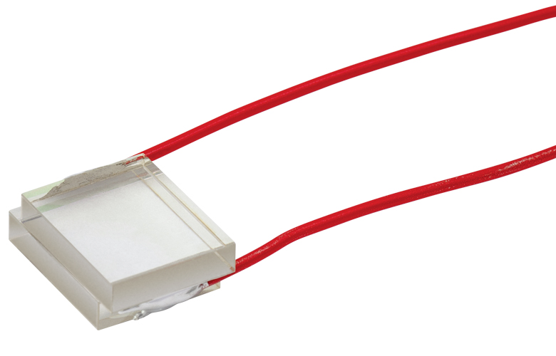
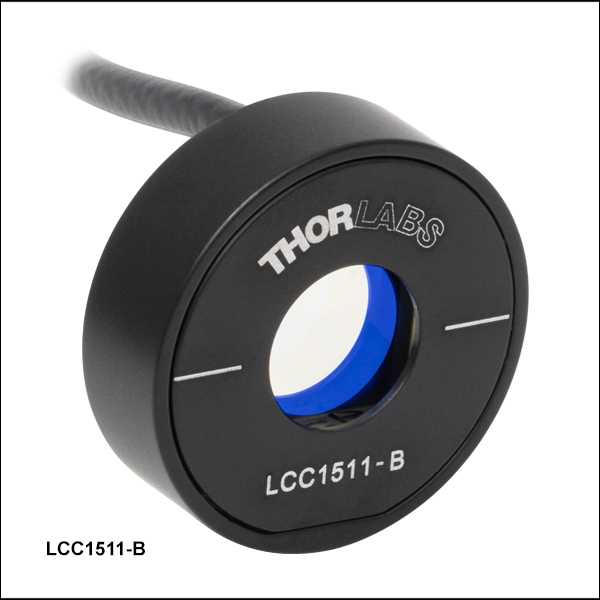
Thorlabs' Ø10 mm clear aperture, compensated, half-wave liquid crystal retarders are available with AR coatings for 350 - 700 nm (LCC1611-A), 650 - 1050 nm (LCC1611-B), or 1050 - 1700 nm (LCC1611-C). The compensator integrated within the retarder enables 0 nm minimal retardation at a specific driving voltage between 5 V and 20 V (please refer to the Performance tab for more information). These retarders have an outer diameter of 1", making them compatible with any of our Ø1" optic mounts for 9 mm thick optics. The slow axis is indicated by an engraved line on the front of the retarder. Additionally, these mounted retarders have a BNC cable which is approximately 930 mm long for the electrical connection. As this retarder has a 1" outer diameter, it can be mounted using the RSP1(/M) Post-Mountable Rotation Mount or the CRM1PT(/M) 30 mm Cage Rotation Mount.
*If your application does not require the fast switching speeds of the LCC1611-x LCVRs, the previous generation Ø10 mm retarders are available by contacting Tech Sales. See the Custom Capabilities tab for details.

 Zoom
Zoom| Key Specificationsa | |||
|---|---|---|---|
| Item # | LCC1511-A | LCC1511-B | LCC1511-C |
| Wavelength Range | 350 - 700 nm | 650 - 1050 nm | 1050 - 1700 nm |
| Retardance Rangeb | ~30 nm to >λ/2 | ||
| Switching Time (Rise/Fall, Typical) |
2.72 ms / 0.16 ms @ 25 °C, 635 nm |
3.41 ms / 0.24 ms @ 25 °C, 780 nm |
21.29 ms / 0.50 ms @ 25 °C, 1550 nm |
| Retardance Uniformity (RMS)c |
<λ/50 @ 400 nm | <λ/50 @ 650nm | <λ/50 @ 1050 nm |
| Surface Quality | 40-20 Scratch-Dig | ||
- Ø10 mm Clear Aperture
- Retardance: ~30 nm to λ/2
- 1" Outer Diameter
- 5 Standard AR Coatings Available
Thorlabs' Ø10 mm clear aperture, uncompensated, half-wave liquid crystal retarders are available with AR coatings for 350 - 700 nm (LCC1511-A), 650 - 1050 nm (LCC1511-B), or 1050 - 1700 nm (LCC1511-C) light. These retarders have an outer diameter of 1", making them compatible with any of our Ø1" optic mounts for 8 mm thick optics. The slow axis is indicated by an engraved line on the front of the retarder. Additionally, these mounted retarders have a 930 mm long BNC cable for the electrical connection. As this retarder has a 1" outer diameter, it can be mounted using the RSP1(/M) Post-Mountable Rotation Mount or the CRM1PT(/M) 30 mm Cage Rotation Mount.
We also offer thermally-stabilized Ø10 mm half-wave LC retarders for constant retardance in changing ambient temperatures.
*If your application does not require the fast switching speeds of the LCC1511-x LCVRs, the previous generation Ø10 mm retarders are available by contacting Tech Sales. See the Custom Capabilities tab for details.

 Zoom
Zoom| Key Specificationsa | ||
|---|---|---|
| Item # | LCC1111-D | LCC1111-MIR |
| Wavelength Range | 1650 - 3000 nm | 3600 - 5600 nm |
| Retardance Rangeb | ~30 nm to >λ/2 | |
| Switching Time (Rise/Fall, Typical) |
192 ms / 1 ms @ 25.6 °C, 2200 nm |
372 ms / 14 ms @ 25.6 °C, 4400 nm |
| Retardance Uniformity (RMS)c |
<λ/30 @ 1650 nm | <λ/10 @ 3600 nm |
| Surface Quality | 60-40 Scratch-Dig | |
- Ø10 mm Clear Aperture
- Retardance: ~30 nm to λ/2
- 1" Outer Diameter
- 2 Standard AR Coatings Available
Thorlabs' Ø10 mm clear aperture, uncompensated, half-wave liquid crystal retarders are available with AR coatings for 1650 - 3000 nm (LCC1111-D) or 3600 - 5600 nm (LCC1111-MIR) light. These retarders have an outer diameter of 1", making them compatible with any of our Ø1" optic mounts for 8 mm thick optics. The slow axis is indicated by an engraved line on the front of the retarder. Additionally, these mounted retarders have a 930 mm long BNC cable for the electrical connection. As this retarder has a 1" outer diameter, it can be mounted using the RSP1(/M) Post-Mountable Rotation Mount or the CRM1PT(/M) 30 mm Cage Rotation Mount.
We also offer thermally-stabilized Ø10 mm half-wave LC retarders for constant retardance in changing ambient temperatures.

 Zoom
Zoom| Key Specificationsa | ||
|---|---|---|
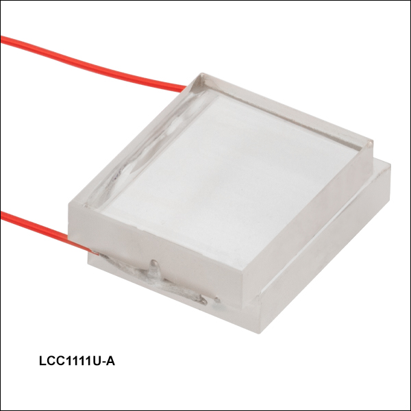
| Item # | LCC1111U-A | LCC1111U-B |
| Wavelength Range | 350 - 700 nm | 650 - 1050 nm |
| Retardance Rangeb | ~30 nm to >λ/2 | |
| Switching Time (Rise/Fall, Typical) |
10.2 ms / 310 µs @ 22 °C, 635 nm |
19.52 ms / 0.44 ms @ 25 °C, 780 nm |
| Retardance Uniformity (RMS)c | <λ/50 @ 400 nm | <λ/50 @ 650 nm |
| Surface Quality | 40-20 Scratch-Dig | |
| Dimensions (L x W x D) |
17.0 mm x 12.0 mm x 6.0 mm (0.67" x 0.47" x 0.24") |
|
- Ø10 mm Clear Aperture
- Retardance: ~30 nm to λ/2
- Dimensional Tolerance: ±0.4 mm
- AR Coated for 350 - 700 nm or 650 - 1050 nm
Thorlabs' Ø10 mm clear aperture, unmounted, uncompensated, half-wave liquid crystal retarders are ideal for specialized applications where space is at a premium. The LCC1111U-A is AR coated for 350 - 700 nm and the LCC1111U-B is AR coated for 650 - 1050 nm. The compact size of these retarders gives the user flexibility for mounting and placement within an existing system for OEM and other specialized applications. The LCC1111U-x unmounted retarders come with attached wires for connecting to a voltage driver and are compatible with our LCC25 and KLC101 LC Controllers sold below.
Custom wavelengths are available with clear apertures of either Ø10 mm or Ø20 mm. If interested in a custom unmounted retarder, please contact Tech Sales for more information.

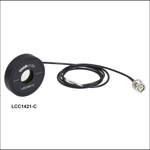 Zoom
Zoom| Key Specificationsa | |||
|---|---|---|---|
| Item # | LCC1421-A | LCC1421-B | LCC1421-C |
| Wavelength Range | 350 - 700 nm | 650 - 1050 nm | 1050 - 1700 nm |
| Retardance Rangeb | 0 nm to >λ/2 | ||
| Switching Time (Rise/Fall, Typical) |
15.8 ms / 260 µs @ 22 °C |
34 ms / 360 µs @ 22 °C |
152 ms / 510 µs @ 25.6 °C |
| Retardance Uniformity (RMS)c |
<λ/20 @ 400 nm | <λ/20 @ 650 nm | <λ/20 @ 1050 nm |
| Surface Quality | 60-40 Scratch-Dig | ||
- Ø20 mm Large Clear Aperture
- Retardance: 0 nm to λ/2
- Compensated for 0 nm Minimum Retardance
- SM2 External Threading
- 3 Standard AR Coatings Available
Thorlabs' Ø20 mm clear aperture, compensated, half-wave liquid crystal retarders are available with AR coatings for 350 - 700 nm (LCC1421-A), 650 - 1050 nm (LCC1421-B), or 1050 - 1700 nm (LCC1421-C). The compensator integrated within the retarder enables 0 nm minimal retardation at a specific driving voltage between 5 V and 20 V (please refer to the Performance tab for more information). These retarders have external SM2 threading, making them compatible with any of our Ø2" threaded optic mounts. This includes mounts like the RSP2, an SM2 mount which provides precise rotational adjustment and post mounting capability, or the LCRM2A which adds 60 mm cage-mounting versatility. The slow axis is indicated by an engraved line on the front of the retarder. Additionally, these mounted retarders have a BNC cable which is approximately 944 mm long for the electrical connection.

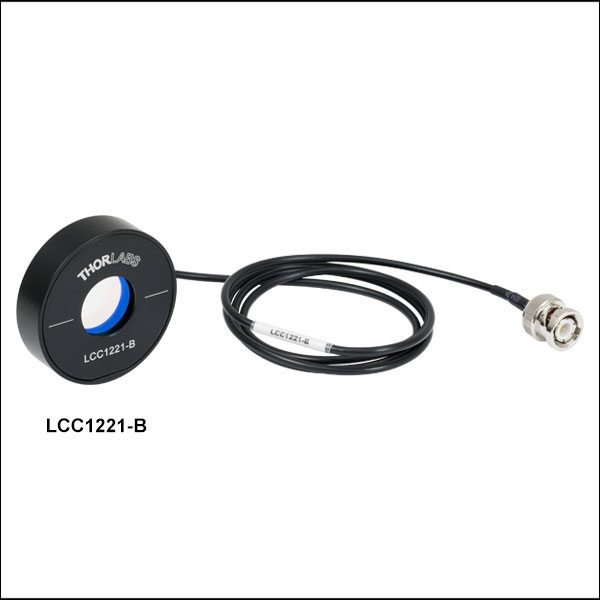 Zoom
Zoom| Key Specificationsa | |||
|---|---|---|---|
| Item # | LCC1221-A | LCC1221-B | LCC1221-C |
| Wavelength Range | 350 - 700 nm | 650 - 1050 nm | 1050 - 1700 nm |
| Retardance Rangeb | ~30 nm to >λ/2 | ||
| Switching Time (Rise/Fall, Typical) |
10.2 ms / 310 µs @ 22 °C |
19.52 ms / 0.44 ms @ 25 °C, 780 nm |
95.8 ms / 1.81 µs @ 25.6 °C |
| Retardance Uniformity (RMS)c |
<λ/50 @ 400 nm | <λ/50 @ 650 nm | <λ/50 @ 1050 nm |
| Surface Quality | 40-20 Scratch-Dig | ||
- Ø20 mm Large Clear Aperture
- Retardance: ~30 nm to λ/2
- 2" Outer Diameter
- 3 Standard AR Coatings Available
Thorlabs' Ø20 mm clear aperture, uncompensated liquid crystal retarders are available with AR coatings for 350 - 700 nm (LCC1221-A), 650 - 1050 nm (LCC1221-B), or 1050 - 1700 nm (LCC1221-C) light. These retarders have an outer diameter of 2", making them compatible with any of our Ø2" optic mounts for 13 mm thick optics. The slow axis is marked by an engraved line on the front of the retarder. Additionally, these mounted retarders have a 940 mm long BNC cable for the electrical connection. As this retarder has a 2" outer diameter, it can be mounted using the RSP2 Post-Mountable Rotation Mount or the LCRM2A 60 mm Cage Plate Rotation Mount.

 Zoom
Zoom
- 0 to ±25 VAC Square-Wave Output Voltage
- LCC25: 2000 ± 5 Hz
- KLC101: Adjustable from 500 Hz to 10 kHz
- Internal and External Options for Modulating the Output Square-Wave Amplitude
- Edit Settings Using Device Panel or Control via USB Input from a PC
The LCC25 and KLC101 Liquid Crystal (LC) Controllers are both designed to operate Thorlabs' liquid crystal cells, rotators, and retarders (except for the LCC2415-VIS, which has an integrated controller). Each controller supplies a a square-wave AC voltage output with an amplitude that can be adjusted from 0 VRMS to ±25 VRMS. Both will automatically detect and correct any DC offset to within ±10 mV in real time, helpful for increasing the life of liquid crystal devices.
LCC25 Benchtop Controller
The LCC25 LC Controller produces a 2000 Hz square-wave AC voltage output. Both the front panel and USB interface allow the user to select two voltage levels, Voltage 1 and Voltage 2. When the LCC25 is operated in the constant voltage mode, the output of the controller will have an amplitude equal to either of the two set voltage levels. In Modulation mode, the amplitude of the 2,000 Hz square-wave output will switch between Voltage 1 and Voltage 2 at a frequency that can be set internally (0.5 Hz to 150 Hz) or triggered externally with a 0 to 5 V TTL input (0.5 Hz to 500 Hz). The LCC25 controller's software package also allows the user to define a voltage sequence by specifying a starting voltage, ending voltage, voltage step size, and dwell time.
Please visit the LCC25 controller page for more information on this controller's features.
KLC101 K-Cube™ Controller
The KLC101 K-Cube™ LC Controller is a part of Thorlabs' growing line of high-end, compact controllers. It supplies a square-wave AC output voltage with a user-set frequency from 500 Hz to 10 kHz and features a small 60.0 mm x 60.0 mm footprint. The controller can store two voltage and frequency combinations, PresetV1 and Preset V2, either of which can be selected as the output. Additionally, the controller top panel, software, and trigger ports allow the use to create customized output voltage sequences. The voltage can be set to switch between PresetV1 and PresetV2 at rates from 0.1 and 150 Hz using the top panel controls or software. When in this mode, one of the trigger ports will output a 5 V logic signal, with the high level indicating that the output is PresetV2 and the low level indicating the output is PresetV1. Alternatively, a trigger port can be used as an input for a 5 V logic signal to switch between PresetV1 and PresetV2. The software also enables Sequence and Sweep Modes. The Sequence tool can be used to set a sequence of output voltage amplitudes, frequencies, and step durations. In Sweep mode, the KLC101 controller will scan between user-set start and end voltages with a user-specified step size and step duration.
Note that the KLC101 controller does not ship with a power supply. For applications requiring a single K-cube, the TPS002 power supply (sold below) can be used. We also offer USB controller hubs for use with multiple K-cubes.
See the full KLC101 controller web presentation for more information on the features of this controller and its power supply options.
| Item # | Adjustable Output Voltage |
Voltage Resolution |
Adjustable Output Frequencya |
Internal Modulationa |
External Modulation |
Slew Rate |
DC Offset |
Warm Up Time |
Output Current (Max) |
External Input Voltage (Max) |
|---|---|---|---|---|---|---|---|---|---|---|
| LCC25 | 0 to ±25 V RMS | 1.0 mV | 2,000 ± 5 Hz | 0.5 to 150 Hz | 0.5 to 500 Hz | 10 V/µs | ±10 mV | 30 Minutes | 15 mA | 5 VDC |
| KLC101 | 500 Hz to 10 kHz | 0.1 to 150 Hz | 150 Hz (Max) | 50 mA |