 Products Home / Actuators, Adjusters, & Transducers / Piezoelectric Chips and Stacks / Co-Fired Piezoelectric Actuators, 4.6 µm to 20.0 µm Travel
Co-Fired Piezoelectric Actuators, 4.6 µm to 20.0 µm Travel
- Free-Stroke Displacement Options from 4.6 µm to 20.0 µm
- In-Stack and On-Stack Insulation Methods
- Sub-Millisecond Response Times with No Load
- Low 75 V or 150 V Maximum Drive Voltage
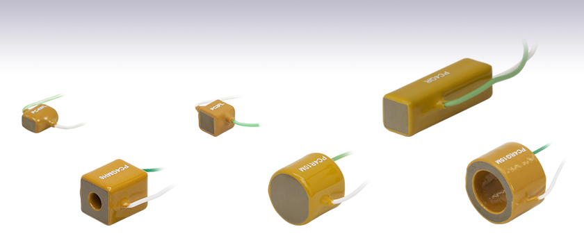
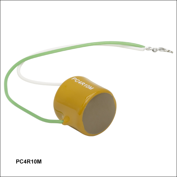
PC4R10M
9.5 µm Stroke
Ø11.0 mm x 10.0 mm
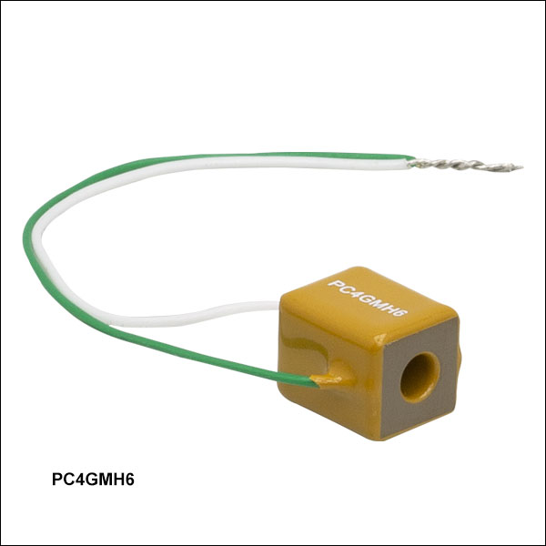
PC4GMH6
9.5 µm Stroke,
8.5 mm x 8.5 mm
x 10.0 mm
PC4QR
20.0 µm Stroke
6.5 mm x 6.5 mm x 20.0 mm
PC4WL
4.6 µm Stroke
3.5 mm x 4.5 mm x 5.0 mm
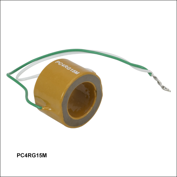
PC4RG15M
9.1 µm Stroke
Ø15.0 mm OD, Ø8.5 mm ID
10.0 mm Long
PC2FL
4.8 µm Stroke
5.0 mm x 5.5 mm x 5.0 mm


Please Wait
| Piezo Selection Guide |
|---|
| Piezoelectric Ceramic Stacks |
| Discrete, Square |
| Discrete, Square with Through Hole |
| Discrete, Round |
| Discrete, Ring |
| Discrete, Hermetically Sealed |
| Discrete, Shear (1D to 3D Positioners) |
| Co-Fired: Square, Square with Through Hole, Round, & Ring |
| Co-Fired or Discrete: Square with Strain Gauges |
| Piezoelectric Crystal Stacks |
| Square |
| Piezoelectric Chips |
| Mounted Piezoelectric Actuators |
| Ultrasonic Piezo Chips & Transducers |
| Vibrating Piezo Actuator |
| Webpage Features | |
|---|---|
| Clicking this icon opens a window containing item-specific specifications. | |


Features
- Epoxy-Coated for Protection Against Rough Handling and Mechanical/Chemical Contamination
- Co-Fired Design Sinters the Stack as a Single Monolithic Unit
- Maximum Displacements from 4.6 µm to 20.0 µm
- 75 V or 150 V Max Drive Voltage
- Square, Square with Through Hole, Round, or Ring Cross-Section
- Fast Response Time: 1/(3×Resonant Frequency)
- Two Different Insulation Methods:
- PC2 Series: Internal Electrodes with Insulation Gap for In-Stack Insulation
- PC4 Series: Internal Electrodes Span Entire Active Cross Section with On-Stack Insulation
Thorlabs' Co-Fired Piezoelectric Actuators are composed of stacked PZT layers separated by electrodes that span the entire surface area of the layer. The entire stack is sintered together into one monolithic structure. These piezoelectric actuators transform electrical energy into precisely controlled mechanical displacements and are ideal for applications requiring rapid, precise positional changes on the nanometer or micrometer scale.
Co-Fired Piezo Stacks differ from Discrete Piezo Stacks in the insulation and conductor design. In the PC4 series co-fired stacks, small amounts of glass filament are precisely located on each side of the stack so that every internal electrode is insulated from the external supply electrode of opposite polarity. This separation enables sequential layers to alternate connections to the positive and negative poles (or applied bias and ground). Compared to using an insulating gap as in discrete stacks and the PC2 series co-fired stacks, this design allows for a higher contact area and percentage of active PZT material, which lends itself to lower internal stress. The in-stack insulation of the PC2 series yields a lower maximum drive voltage of 75 V. For more details and a diagram further comparing the two piezo stack insulation methods, please refer to the Operation tab.
These multilayer devices are ideal for nano- and micro-positioning. As the voltage applied to the actuator goes from 0 V to the maximum drive voltage, the piezo expands longitudinally. These open-loop piezoelectric actuators offer maximum displacements from 4.6 µm to 20.0 µm. Piezoelectric devices, such as these actuators, exhibit hysteresis, thus the displacement of the actuator is not solely based on applied voltage. When it is necessary to precisely track the displacement of the actuator, Thorlabs recommends our piezo stack actuators with attached strain gauges.
Thorlabs' piezoelectric chips are individually inspected using a proprietary AI algorithm to ensure the highest quality of our line of piezo chips, actuators, and transducers.
Integration
Our PC2 Series and PC4 Series Piezo Stacks are compatible with hemispheres and end cups to minimize internal stress when mounting. Please refer to the info icons ![]() )
)
The green lead on the piezoelectric actuator must be connected to the high side of the voltage source used to drive the actuator. Do not drive the piezoelectric actuator with a reverse bias voltage, as this could destroy the device. Piezoelectric actuators should not be used in liquid, in the presence of combustible gases or liquids, or cleaned with organic solvents.
Caution: After driving, the piezo is fully charged. Directly connecting the green and white wires has the risk of electricity discharging, spark, and even failure. We recommend using a resistor (>1 kΩ) between the green and white wires to release the charge.
Thorlabs also offers an expanding line of 75 V, 100 V, and 150 V piezoelectric stacks and chips, including discrete piezo stacks with 5.2 µm - 100.0 µm travel and piezo chips with 0.7 - 3.6 µm travel, which are ideally suited for OEM applications. For applications requiring larger displacements, we offer amplified piezo actuators with 220 µm - 2500 µm travel.
Operation Notes

Click to Enlarge
Figure 2.1 Diagram of Piezo Stack Insulation Methods:
(a) In-Chip Insulation Used in Chips and Discrete Stacks,
(b) In-Stack Insulation Used in Co-Fired Stacks,
(c) On-Stack Insulation Used in Co-Fired Stacks
Co-Fired Piezo Chips, Co-Fired Piezo Stacks, and Discrete Piezo Stacks
Generally speaking, Thorlabs' co-fired piezo chips and stacks are constructed similarly. In both cases, a structure is built up from alternating electrode layers and green-state lead zirconate titanate (PZT) piezoelectric layers. (The co-fired piezo chips are also available with BiScO3-PbTiO3 (BSPT) piezoelectric layers for higher temperature applications.) The assembled structure is then sintered into a single monolithic unit. Supply electrodes of opposite polarity are attached to opposite sides of the structure. Each internal electrode is electrically coupled to one or the other supply electrode, such that no two adjacent internal electrodes have the same polarity. The most significant differences between the co-fired chips, the PC2 series of co-fired stacks, and the PC4 series of co-fired stacks arise from the way each internal electrode is electrically isolated from the supply electrodes of opposite polarity. The different electrical insulation approaches influence the mechanical properties of the actuators. Actuators fabricated using the three different approaches are diagrammed in Figure 2.1.
In the case of the chips (In-Chip Insulation), the internal electrodes of opposite polarities alternate. Each internal electrode layer is shorter than the full width of the piezo layer. All electrodes of one polarity have edges that are flush with one side of the chip, and all electrodes with the opposite polarity are flush with the opposite side of the chip. Because the electrode does not extend all the way to the opposite edge, the far end of the electrode is completely surrounded by PZT or BSPT material. The PZT or BSPT material enclosing the end of the electrode is insulating, which electrically isolates this electrode from the supply electrode of opposite polarity. This approach to electrically insulating the electrodes creates a region of stress at the edge of the electrode. The stress arises both due the abrupt change in thickness on either side of the electrode edge, as well as the tensile stress created when the PZT or BSPT material sandwiched between electrodes responds to an applied voltage drive signal, but the insulating PZT or BSPT material beyond the edge of the electrodes does not. This stress limits the maximum height of chips manufactured using this approach. The height of chips are limited to ensure internal stresses are low and do not affect lifetime or performance. Chips are sealed in a ceramic layer that offers superior resistance to humidity and heat than epoxy resin coatings.
One way of increasing the height, and therefore the maximum stroke, of piezo actuators based on these chips is to fabricate discrete piezo stacks. These are manufactured by bonding multiple chips together in series using a glass-bead epoxy. Discrete stacks can be fabricated to substantially longer lengths than co-fired chips or stacks, and this allows them to achieve higher maximum displacements while maintaining sub-millisecond response times and a low drive voltage range. As the constituent chips are sealed within a ceramic barrier layer, discrete stacks have superior resistance to humidity and heat than co-fired stacks, which are sealed in an epoxy resin coating.
In the case of the PC2 series of co-fired stacks (In-Stack Insulation), internal electrodes of opposite polarities alternate, much like the piezo chips, with only the middle portions reaching the side of the stacks. The insulation gap of PZT material used in the piezo chips remains, but is included on both sides with only a narrow electrode remaining. This helps increase the stacks lifespan, with narrower electrodes leading to longer lifetimes. Slots are introduced along the length of the stack to help alleviate the mechanical stress caused by the insulating PZT material.
In the case of the PC4 series co-fired stacks (On-Stack Insulation), the electrodes extend across the full width of the PZT layers. The edges of the electrodes are flush with all four sides of the stack, including the side with the supply electrode of opposite polarity. The edge of the internal electrode is insulated from that supply electrode by a layer of glass filament applied to the side of the stack. Precision localized application of the glass filament ensures that the electrode edge is electrically isolated from the supply electrode, and that the filament is applied over minimal surface area; the ability of the supply electrode to make electrical connections to the desired internal electrodes is not affected, and the small amount of applied glass filament does not affect the operation of the actuator. With their full-width electrodes, piezo actuators made using this insulating approach are characterized by homogeneous internal stress. Co-fired stacks can therefore be fabricated with greater heights than chips fabricated using the in-chip insulation approach. Co-fired stacks also have a higher percentage of active PZT material than the discrete stacks, which include inactive bonding layers of glass-bead epoxy. They are coated in an epoxy resin.
Power Connections
A positive bias should be applied across the device using the wires connected to the electrodes. The positive wire should receive positive bias, and the other wire should be connected to ground. Applying a negative bias across the device may cause mechanical failure. The positive wire is either red or green, while the ground wire is white.
Caution: After driving, the piezo is fully charged. Directly connecting the green and white wires has the risk of electricity discharging, spark, and even failure. We recommend using a resistor (>1 kΩ) between the green and white wires to release the charge.
Interfacing a Piezoelectric Stack with a Load
Piezoceramics are brittle and have low tensile strength. Avoid loading conditions that subject the actuator to lateral, transverse, or bending forces. When applied incorrectly, an external load that may appear to be compressive can, through bending moments, cause high tensile stresses within the piezoelectric device. Improperly mounting a load to the piezoelectric actuator can easily result in internal stresses that will damage the actuator. To avoid this, the piezoelectric actuator should be interfaced with an external load such that the induced force is directed along the actuator's axis of displacement. The load should be centered on and applied uniformly over as much of the actuator's mounting surface as possible. When interfacing the flat surface of a load with an actuator capped with a flat mounting surface, ensure the two surfaces are highly flat and smooth and that there is good parallelism between the two when they are mated. If the external load is directed at an angle to the actuator's axis of displacement, use an actuator fitted with a hemispherical end plate or a flexure joint to achieve safe loading of the piezoelectric stack.
To attach a load to co-fired PZT piezo stacks, we recommend using an epoxy that cures at a temperature lower than 80 °C (176 °F), such as our 353NDPK or TS10 epoxies or Loctite® Hysol® 9340. Loads should be mounted only to the translating, uncoated faces of the piezoelectric stack; the coated sides of our co-fired piezo stacks do not translate, and mounting a load to a non-translating face may lead to the mechanical failure of the actuator. Our PC4 Series Piezo Stacks are compatible with hemispheres and end cups to minimize internal stress when mounting. Please refer to the info icons (![]() ) for item-specific compatibility. Some correct and incorrect approaches to interfacing loads with piezoelectric stacks fitted with end plates are discussed in the following.
) for item-specific compatibility. Some correct and incorrect approaches to interfacing loads with piezoelectric stacks fitted with end plates are discussed in the following.
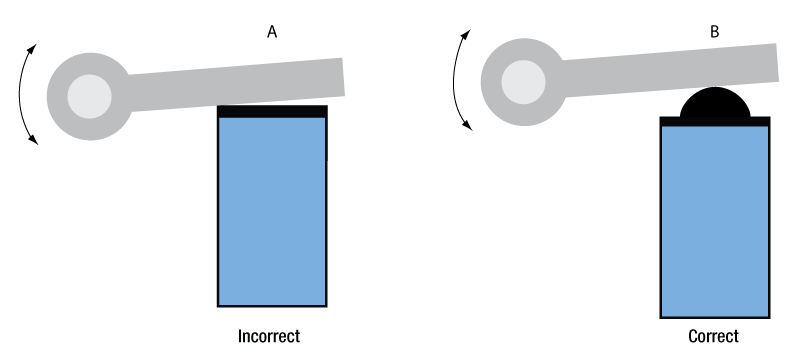
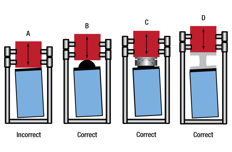
Click to Enlarge
Figure 2.2 Actuation of a lever arm using stack fitted with a flat plate (A, Incorrect), and a hemispherical plate (B, Correct).
Click to Enlarge
Figure 2.3 Loads properly and improperly mounted to PZT actuators using a variety of interfacing methods.
Figure 2.2 presents incorrect (A) and correct (B) methods for using a piezoelectric stack to actuate a lever arm. The correct method uses a hemispherical end plate so that, regardless of the angle of the lever arm, the force exerted is always directed along the translational axis of the actuator. The incorrect interfacing of the stack and the lever arm (A) endangers the stack by applying the full force of the load to one edge of the stack. This uneven loading causes dangerous stresses in the actuator, including a bending moment around the base.
Figure 2.3 shows one incorrect (A) and three correct approaches for interfacing a flat-bottomed, off-axis load with a piezoelectric stack. Approaches A and B are similar to the incorrect and correct approaches, respectively, shown in Figure 2.2. Correct approach C shows a conical end cup, such as the PKFCUP, acting as an interface. The flat surface is affixed to the mating surface of the load, and the concave surface fits over the hemispherical dome of the end plate. In the case of correct approach D, a flexure mount acts as an interface between the off-axis flat mounting surface of the load and the flat mounting plate of the actuator. The flexure mount ensures that the load is both uniformly distributed over the surface plate of the actuator and that the loading force is directed along the translational axis of the actuator.
Operating Under High-Frequency Dynamic Conditions
It may be necessary to implement an external temperature-control system to cool the device when it is operated at high frequencies. High-frequency operation causes the internal temperature of the piezoelectric device to rise. The dependence of the device temperature on the drive voltage frequency for select products can be found in the Spec Sheet accessed by clicking the red docs icon (![]() ) below. The temperature of the device should not be allowed to exceed its specified maximum operating temperature.
) below. The temperature of the device should not be allowed to exceed its specified maximum operating temperature.
Estimating the Resonant Frequency for a Given Applied Load
A parameter of significance to many applications is the rate at which the piezoelectric actuator changes its length. This dimensional rate of change depends on a number of factors, including the bandwidth of the piezoelectric actuator (its resonant frequency), the absolute maximum bandwidth of the driver (its slew rate), the maximum current the piezoelectric device can produce, the capacitance of the piezoelectric stack, and the amplitude of the driving signal. The length of the voltage-induced extension is a function of the amplitude of the applied voltage driving the actuator and the length of the piezoelectric stack. The higher the capacitance, the slower the dimensional change of the actuator.
Quick changes in the applied voltage result in fast dimensional changes to the piezoelectric stack. The magnitude of the applied voltage determines the nominal extension of the stack. Assuming the driving voltage signal resembles a step function, the minimum time, Tmin, required for the length of the actuator to transition between its initial and final values is approximately 1/3 the period of resonant frequency. If there is no load applied to the piezoelectric stack, its resonant frequency is ƒo and its minimum response time is:

After reaching this nominal extension, there will follow a damped oscillation in the length of the actuator around this position. Controls can be implemented to mitigate this oscillation, but doing so may slow the response of the actuator.
Applying a load to the actuator will reduce the resonant frequency of the piezoelectric stack. Given the unloaded resonant frequency of the actuator, the mass of the stack, m, and the mass of the load, M, the loaded resonant frequency (ƒo') may be estimated:
| Posted Comments: | |
Zheng Rong Guo
(posted 2025-05-11 23:50:32.41) Asked 3 questions about PC4QM piezoelectric d33 and S33 and density. jdelia
(posted 2025-05-13 09:21:19.0) Thank you for your inquiry. Our PRC technical support team has been in touch with you with further information to resolve your issue. Jerard Vincent Rubio Ang
(posted 2024-06-21 13:29:35.873) I have the PC4WL, however the design compared to the old product is quite inconvenient since the wires are sticking out to the side. Could I bend the wires straight to be parallel with the piezo without damaging the joint? cdolbashian
(posted 2024-07-01 01:39:19.0) Thank you for contacting Thorlabs. We will contact you directly to to discuss your application. Adolf Canillas
(posted 2020-03-04 06:32:13.32) Hi. I have PC4QR piezoelectric actuators, could you please tell me the thickness of an individual chip (0.1 mm?) and the kind of PZT used (THP42...)? nbayconich
(posted 2020-03-05 02:22:23.0) Thank you for contacting Thorlabs. PC4QR is a co-Fired piezo, we use hundreds of ceramic films during manufacturing. The thickness of these films is about 0.1mm. The PZT material THP51 is used in these actuators. peter.staaf
(posted 2017-04-27 10:53:16.663) Hi
Are there any official insulation properties between endcaps and terminals? A cad drawing of just those parts would be helpful to determine insulation. nbayconich
(posted 2017-05-17 05:46:08.0) Thank you for contacting Thorlabs. The top and bottom end caps of these actuators are inactive piezoelectric material. This is the same material used for the stack but without the electrodes with a typical thickness of 1-1.5mm. A techsupport representative will contact you directly with more information. user
(posted 2017-01-08 22:05:14.633) Hello.
I have 2 questions about PZS001.
1)What is the response time of it?
2)what is d33 and s33 of it? (piezoelectric material specification)
thank you.
best regards. tfrisch
(posted 2017-01-11 10:31:17.0) Hello. Thank you for contacting Thorlabs. The response time will be limited by the feedback loop for closed loop applications, and for open loop, you can see the Piezo Bandwidth tab for details on the expected response. I will reach out to you directly about the material specifications. everardo_flores
(posted 2014-03-27 20:56:42.24) Which is the resolution (in nm) of the PZS001 used with the T-Cube (TPZ001). Thanks! msoulby
(posted 2014-03-28 09:54:18.0) Response from Mike at Thorlabs: The resolution of these actuators is largely dependent on the voltage source that you use. Ideally you would use a high voltage source that has low voltage noise; generally the lower this noise the better the resolution. With our TPZ001 controller, which has a noise value of <2mVRMS you will be able to achieve around 20-30nm of resolution if operated in open loop mode. However in open loop mode with no strain gauge feedback the piezo will likely drift over time. By using the strain gauge with our TSG001 reader you will be able to remove this drift and also improve you resolution by a factor of 2 or 3. sjf1e12
(posted 2013-07-17 12:30:26.94) I'm looking to buy a piezoelectric actuator. I want to actuate it at up to around 100kHz. Is it required to use a specialist piezo controller, also available from this site? If we have a function generator and a power source could we control it using this?
Many thanks cdaly
(posted 2013-07-18 15:57:00.0) Response from Chris at Thorlabs: Thank you for your feedback. No special controller is required. It's just a matter of applying a voltage across the leads, so any modulated voltage source can be used that matched the necessary specs. The issue is going to be the slew rate of your setup. The AE0203D04F can be driven at 100kHz, but the limiting factor is going to be the max current output of your source. A larger displacement is going to require a larger current. For example if you want to drive at 100kHz at the full range of 0-150V, you are going to need a source which can output around 2.7A max current. And can be modulated between 0-150V at 100kHz. These will scale linearly with the max voltage/displacement you choose, so for example if you were only going up to 50V, 0.9A would be the max required current. Please note that the resonant frequency for this actuator is 261 kHz, but this will decease as load is added. hadmack
(posted 2013-07-10 19:24:21.967) Do you stock the NEC AE1010D16F piezo as well? Can I special order this? jlow
(posted 2013-07-11 08:19:00.0) Response from Jeremy at Thorlabs: The AE1010D16F is not a piezo that we stock. We will get in contact with you on special ordering this. jlow
(posted 2013-01-14 13:44:00.0) Response from Jeremy at Thorlabs: The spec sheet for the AE0505D18F can be found at http://www.thorlabs.com/Thorcat/8600/AE0505D18F-SpecSheet.pdf. The maximum drive voltage for this is +100V. Do not apply a negative voltage to this. The resonant frequency is dependent on the mechanical load that you are putting on the piezo. With no mechanical load, the resonant frequency is at 69kHz. The piezo bandwidth will most likely be limited by the slew rate of the driver. We have a small tutorial for this located at http://www.thorlabs.com/NewGroupPage9.cfm?ObjectGroup_ID=61, under the "Piezo Bandwidth" tab. eomjonghyun
(posted 2013-01-11 01:31:36.36) Hi My name is Jeremy belonging into GIST in Korea.
I am testing the vibration of PZT. I have PZT, the model number is AE0505D18F.
I drive this PZT with AC signal from my function generator and PZT driver(MDT694A). I wonder which conditions driving PZT are required, such as frequency, dirving voltage(for PZT diriver and Vpeak of AC signal from function generator)
Would you recommend the appropriate conditions for PZT driving?
Best,
Jeremy jjurado
(posted 2011-08-17 09:15:00.0) Response from Javier at Thorlabs to last poster: We currently do not have experimental data regarding the minimum achievable incremental movement that can be achieved when using the PZS001 piezo stack with the AMP001 amplifier and the TSG001 strain gauge reader. Testing this would require measurement equipment with resolution better than the nanometer-level feedback that can be achieved with the TSG001. Please contact us at techsupport@thorlabs.com if you have any further questions or comments. user
(posted 2011-08-11 11:49:04.0) What is the minimum displacement that strain guage can measure for PZS001. (Using AMP001 & TSG001). jjurado
(posted 2011-02-25 10:05:00.0) Response from Javier at Thorlabs to hadmack: Thank you for submitting your request. Our piezo stacks are not rated for operation in vacuum, and we currently cannot offer special vacuum-compatible versions. Eegarding the strain gauge feedback, it is not recommended to wire two gauges in parallel, as it would not be possible to get a stable feedback from such a system. However, you could use use one strain gage and have one piezo act as the closed feedback loop and the other stack as a slave. I will contact you directly for further support. hadmack
(posted 2011-02-23 23:31:35.0) Are these piezo stacks vacuum compatible? Is it possible to order a vacuum compatible version?
Do you offer any smaller piezos with a strain gauge?
If I need double the 17um range of the PZS001 I could stack two in series and wire in parallel. But what about the strain gauges? Can these be wired in parallel as well or should I only employ one piezo for half of the total stack and allow this to compensate the linearity of the combined stack?
Thanks. Thorlabs
(posted 2010-12-07 10:13:43.0) Response from Javier at Thorlabs to qinyanding: The PZS001 uses an AE0505D16F piezo electric actuator. You can click on the "Specs" tab to view all the specs for this item. I will contact you directly in case you have any additional questions. qinyanding
(posted 2010-12-07 11:05:55.0) Ive got three PZS001 for my laborary. As I want to do some simulation about the piezo stack together with my application, I need to know all the specifications and parameters about the piezo material.
Would you please do me a favor by telling me the material of PZS001, so that I can look its parameters up in our database? Or, if possible, would you please directly send me all the piezo parameters?
Thanks! TechnicalMarketing
(posted 2007-10-17 10:59:32.0) Thank you for informing us of the difficulties you had when looking for piezo stacks. We have implemented some changes that should make this easier. Please feel free to contact us if you have any further issues. acable
(posted 2007-10-15 16:39:38.0) When i searched on "piezo stack" these products didnt come up. I then guessed at the part number and got the search result to send me to the last page for that product (the page that comes up when i click on the part number in the price box). My problem was that i then didnt see a "View Other Products in this Family" link, i had to go out and come through the visual navigation which is a lot of clicks. technicalmarketing
(posted 2007-09-10 10:35:58.0) Dear hrglnabi
In order to monitor the strain gauge on the PZS001 with the TSG001 you need an amplification circuit. Thorlabs has recently released an AMP001 amplification circuit for this purpose. The AMP001 web presentation has not been completed yet, but information about the product can be found on page 403 of the volume 19 catalog and the part can be purchased by contacting one of our sales representatives. The manual included with the AMP001 includes a circuit schematic detailing how to connect the PZS001 to the TSG001 with the use of the AMP001. hrglnabi
(posted 2007-09-09 10:37:08.0) Dear Sir/Madam
Is there any documentation that clearly explains how to connect the PZS001 to TSG001.
Thanks norman.lippok
(posted 2007-08-30 22:44:33.0) How accurate can the AE0505D18 Piezo be employed? How much displacement for 1V...is it 0.15um/V? Whats the smallest displacement for this Piezo?
Thank you. |

 Zoom
Zoom- Square Cross-Section Using In-Stack Insulation
- Max Drive Voltage: 75 V
- Length Tolerance: ±5 µm
- Operating Temperature: -25 to 110 °C
| Item #a | Info | Displacement (Free Stroke)b |
Stack Dimensionsc | Resonant Frequencyd |
Recommended Preloade |
Capacitancef | Blocking Force @ 75 V |
|---|---|---|---|---|---|---|---|
| PC2FL | 4.8 µm ± 15% | <200 N (<45 lbs) | 860 nF ± 15% | 500 N (110 lbs) | |||
| PC2QM | 9.5 µm ± 15% | 6.5 mm x 7.0 mmg x 10.0 mm | 105 kHz ± 10% | <400 N (<90 lbs) | 3.5 µF ± 15% | 1000 N (220 lbs) |

 Zoom
Zoom- Square Cross-Section Using On-Stack Insulation
- Max Drive Voltage: 150 V
- Length Tolerance: ±5 µm
- Operating Temperature: -25 to 110 °C
| Item #a | Info | Displacement (Free Stroke)b |
Stack Dimensionsc | Resonant Frequencyd |
Recommended Preloade |
Capacitancef | Blocking Force @ 150 V |
|---|---|---|---|---|---|---|---|
| PC4WL | 4.6 µm ± 15% | 3.5 mm x 4.5 mm x 5.0 mm | <100 N (<22.5 lbs) | 60 nF ± 15% | 250 N (55 lbs) | ||
| PC4FL | 4.6 µm ± 15% | <200 N (<45 lbs) | 125 nF ± 15% | 500 N (110 lbs) | |||
| PC4QM | <400 N (<90 lbs) | 650 nF ± 15% | |||||
| PC4WM | 9.5 µm ± 15% | 3.5 mm x 4.5 mm x 10.0 mm | 115 kHz ± 10% | <100 N (<22.5 lbs) | 180 nF ± 15% | 250 N (55 lbs) | |
| PC4QQ | 18.0 µm ± 12% | 6.5 mm x 6.5 mm x 18.0 mm | 65 kHz ± 10% | <400 N (<90 lbs) | 1350 nF ± 15% | 1000 N (220 lbs) | |
| PC4GQ | 19.0 µm ± 11% | 8.5 mm x 8.5 mm x 18.0 mm | 64 kHz ± 10% | <800 N (<180 lbs) | 2500 nF ± 15% | 2000 N (440 lbs) | |
| PC4QR | 20.0 µm ± 11% | 6.5 mm x 6.5 mm x 20.0 mm | 59 kHz ± 10% | <400 N (<90 lbs) | 1400 nF ± 15% | 1000 N (220 lbs) | |
| PC4GR | 20.0 µm ± 11% | 8.5 mm x 8.5 mm x 20.0 mm | 59 kHz ± 10% | <800 N (<180 lbs) | 2800 nF ± 15% | 2000 N (440 lbs) |

 Zoom
Zoom- Square Cross-Section with Ø2.5 mm Through Hole (+1.0/-0 mm Diameter Tolerance)
- Max Drive Voltage: 150 V
- Length Tolerance: ±5 µm
- Operating Temperature: -25 to 110 °C
| Item #a | Info | Displacement (Free Stroke)b |
Stack Dimensionsc | Resonant Frequencyd |
Recommended Preloade |
Capacitancef | Blocking Force @ 150 V |
|---|---|---|---|---|---|---|---|
| PC4GMH6 | 9.5 µm ± 15% | 8.5 mm x 8.5 mm x 10.0 mm | 107 kHz | <700 N (160 lbs) | 1.00 µF ± 15% | 1750 N (400 lbs) |

 Zoom
Zoom- Round Cross-Section
- Max Drive Voltage: 150 V
- Length Tolerance: ±5 µm
- Operating Temperature: -25 to 110 °C
| Item #a | Info | Displacement (Free Stroke)b |
Stack Dimensionsc | Resonant Frequencyd |
Recommended Preloade |
Capacitancef | Blocking Force @ 150 V |
|---|---|---|---|---|---|---|---|
| PC4R10M | 9.5 µm ± 15% | Ø11.0 mm x 10.0 mm | 104 kHz ± 10% | <1200 N (270 lbs) | 1.95 µF ± 15% | 3000 N (675 lbs) |

 Zoom
Zoom- Ring Cross-Section with Ø8.5 mm Inner Diameter
- Max Drive Voltage: 150 V
- Length Tolerance: ±5 µm
- Operating Temperature: -25 to 110 °C
| Item #a | Info | Displacement (Free Stroke)b |
Stack Dimensionsc | Resonant Frequencyd |
Recommended Preloade |
Capacitancef | Blocking Force @ 150 V |
|---|---|---|---|---|---|---|---|
| PC4RG15M | 9.1 µm ± 15% | Outer Diameter: 15.0 +0/-0.5 mm Inner Diameter (Min): 8.5 mm Length: 10.0 mm ± 5 μm |
137 kHz ± 10% | <1000 N (220 lbs) | 1.50 µF ± 15% | 2500 N (550 lbs) |