 Products Home / Actuators, Adjusters, & Transducers / Piezoelectric Chips and Stacks / Discrete Piezoelectric Stacks with Through Hole, 7.0 µm to 40.0 µm Travel
Discrete Piezoelectric Stacks with Through Hole, 7.0 µm to 40.0 µm Travel
- Low-Voltage Piezo Stack with 150 V Max Voltage
- Sub-Millisecond Response Time
- Ø2.0 mm or Ø3.0 mm Central Through Hole
- 7.0 µm, 20.0 µm, or 40.0 µm Maximum Free Stroke Displacement
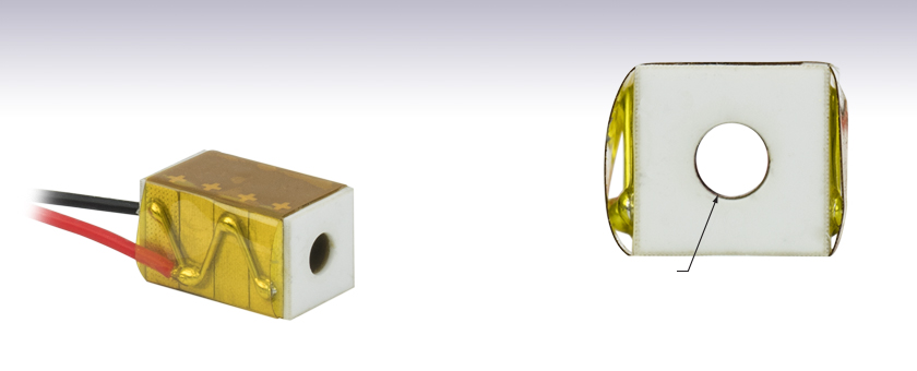
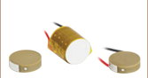
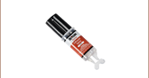
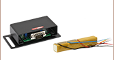
PK4FA2H3P2
150 V Piezo Stack with Two Flat Ceramic End Plates
Central Ø2 mm
Through Hole
Front View of the PK4FA2H3P2


Please Wait
| Piezo Selection Guide |
|---|
| Piezoelectric Ceramic Stacks |
| Discrete, Square |
| Discrete, Square with Through Hole |
| Discrete, Round |
| Discrete, Ring |
| Discrete, Hermetically Sealed |
| Discrete, Shear (1D to 3D Positioners) |
| Co-Fired: Square, Square with Through Hole, Round, & Ring |
| Co-Fired or Discrete: Square with Strain Gauges |
| Piezoelectric Crystal Stacks |
| Square |
| Piezoelectric Chips |
| Mounted Piezoelectric Actuators |
| Ultrasonic Piezo Chips & Transducers |
| Vibrating Piezo Actuator |
| Webpage Features | |
|---|---|
| Clicking this icon below will open a window that contains specifications, mechanical drawings, and graphs. | |

Features
- 0 to 150 V Drive Voltage Range
- Four Versions Available
- 7.0 µm Free Stroke Displacement with Ø2.0 mm Through Hole
- 20.0 µm Free Stroke Displacement with Ø2.0 mm Through Hole
- 40.0 µm Free Stroke Displacement with Ø2.0 mm Through Hole
- 40.0 µm Free Stroke Displacement with Ø3.0 mm Through Hole
- Custom Options Available; Please Contact Tech Support
- For Use in Open-Loop Setups
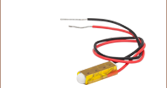
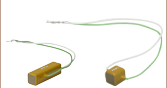
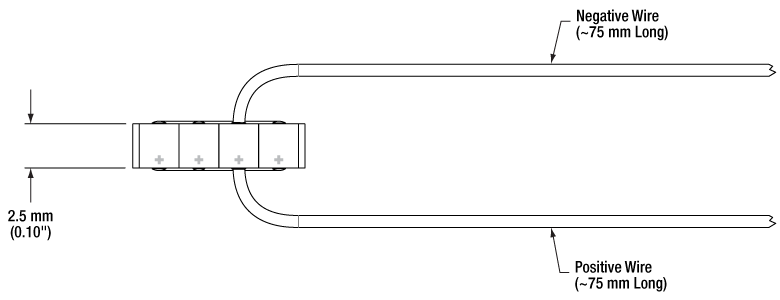
- Pre-Attached Wires (~75 mm Long) for Ease of Integration
- Ideal for OEM Applications
- Flat End Plates Assist in Distribution of Applied Force
Thorlabs' Discrete Piezoelectric Stacks consist of multiple piezoelectric chips, each with a central through hole, stacked face-to-face and bonded via epoxy and glass beads. By combining many chips, a stack is able to achieve a free stroke displacement that is significantly larger than that of its single chip counterpart while maintaining sub-millisecond response times and a low drive voltage range. The central through hole makes these piezos ideal for laser tuning and micro-dispensing applications.
Flat ceramic plates with matching through holes cap the two mounting surfaces on opposite ends of the piezoelectric stack. The ceramic plates assist in both distributing the applied force of the load over the mounting surface of the stack and in directing the force along the actuator's axis of translation. When interfacing the flat surface of a load with this flat mounting surface, ensure the two surfaces are highly flat and smooth and that there is good parallelism between the two when they are mated. For more details see the Operation tab.
Thorlabs' piezoelectric chips are individually inspected using a proprietary AI algorithm to ensure the highest quality of our line of piezo chips, actuators, and transducers.
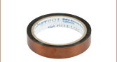
A ceramic layer covering the other four sides and central hole of the stack acts as a barrier against moisture. The ceramic layer offers better protection against moisture than an epoxy coating. For convenience, the stacks have pre-attached 75 mm long wires and are wrapped in polyimide tape. Piezo chips with custom dimensions, voltage ranges, and coatings are available. Please contact Tech Support for more information.
Our piezoelectric tutorial contains more information about the design and function of piezoelectric stacks.

Click to Enlarge
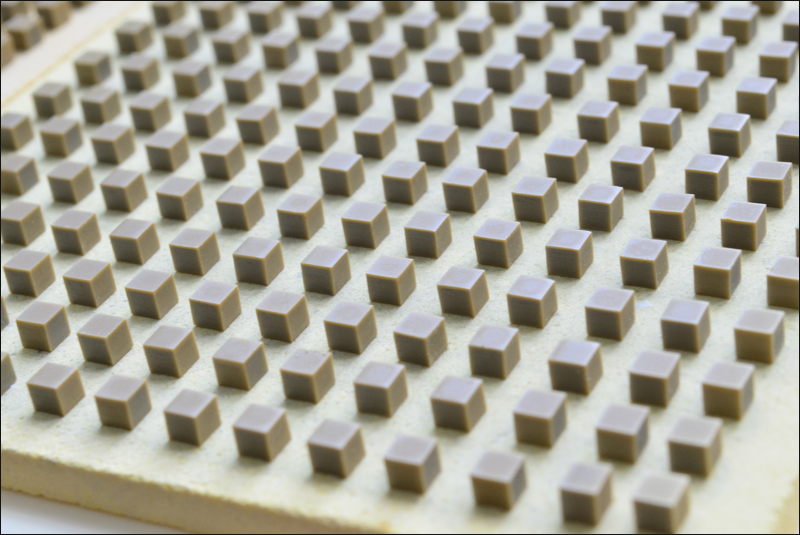
Dicing the PZT Block into Individual Elements
Click to Enlarge
Chips After Binder Burnout and Sintering
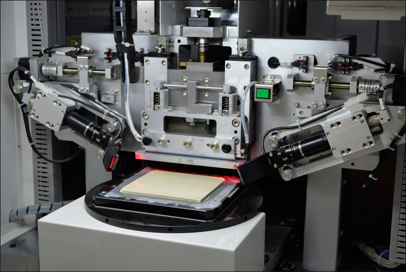
Thorlabs' In-House Piezoelectric Manufacturing
Our piezoelectric chips are fabricated in our production facility in China, giving us full control over each step of the manufacturing process. This allows us to economically produce high-quality products, including custom and OEM devices. A glimpse into the fabrication of our piezoelectric chips follows. For more information about our manufacturing process and capabilities, please see our Piezoelectric Capabilities page.
- Build Blocks from Flexible Sheets of Lead Zirconate Titanate (PZT) or BiScO3-PbTiO3 (BSPT) Powder
- Screen Print Electrodes on Each Individual Sheet
- Layer the Printed Sheets One Top of Another
- Consolidate the Layered Sheets in an Isostatic Press
- Dice the Block into Individual Elements
- Purge Solvent and Binder Material Residues by Heat Treating the Elements
- Sinter the Elements to Fuse the Piezoelectric Pressed Powder and Grow PZT or BSPT Crystals
- Lap the Elements to Achieve Tight Dimensional Tolerances: ±5 µm for Each Element
- Screen Print the Outer Electrodes on the Elements
- Align the Individual PZT or BSPT Crystals Along the Same Axis by Poling the Elements
Click to Enlarge
Figure 2.1 Schematic of PK4DMP2 Piezo Stack
Operation Notes
Power Connections
A positive bias should be applied across the device using the wires connected to the electrodes. The positive wire should receive positive bias, and the other wire should be connected to ground. Applying a negative bias across the device may cause mechanical failure. The positive wire may be identified in two ways: it is red, as can be seen in the product images, and it is attached to electrodes on the side of the stack indicated by the line of + marks, as is depicted in Figure 2.1. (On some devices, the line of + marks is replaced with a line of dots.) The wire that should be grounded is black, and it is attached to the electrodes on the side of the stack opposite the side with the positive electrodes.
Caution: after driving, the piezo is fully charged. Directly connecting the positive and negative electrodes has the risk of electricity discharging, spark, and even failure. We recommend using a resistor (>1 kΩ) between the wires to release the charge.
Preloading
The maximum displacement of these actuators is achieved when they are preloaded with the maximum displacement load, which is specified for each product. The actual value of the maximum displacement varies for each item and must be experimentally determined; however, the maximum displacement will always be larger than the free stroke displacement. Preloading increases the length of the actuator's stroke because the poling process performed during fabrication does not align all ferroelectric grains in the piezoelectric material in the same direction. Preloading the actuator mechanically forces many of the mis-aligned grains into a more ideal alignment. Applying a driving voltage across the piezo material causes the orientations of the ferroelectric grains to rotate so they become aligned with the applied field, and this results in a dimensional change of the piezo material. When more ferroelectric grains are initially aligned in the same direction, the dimensional change of the piezo material in response to the applied driving voltage is greater. Preloads greater than the optimal maximum displacement load result in displacements less than the maximum displacement, as higher loads oppose the switching of the grain orientations in response to the applied driving voltage.
Soldering Wire Leads to the Electrodes
If wire leads must be reattached to the electrodes, a soldering temperature no higher than 370 °C (700 °F) should be used, and heat should be applied to each electrode for a maximum of 2 seconds. Solder the lead to the middle of the electrode and keep the region over which heat is applied as small as possible.
Interfacing a Piezoelectric Stack with a Load
Piezoceramics are brittle and have low tensile strength. Avoid loading conditions that subject the actuator to lateral, transverse, or bending forces. When applied incorrectly, an external load that may appear to be compressive can, through bending moments, cause high tensile stresses within the piezoelectric device. Improperly mounting a load to the piezoelectric actuator can easily result in internal stresses that will damage the actuator. To avoid this, the piezoelectric actuator should be interfaced with an external load such that the induced force is directed along the actuator's axis of displacement. The load should be centered on and applied uniformly over as much of the actuator's mounting surface as possible. When interfacing the flat surface of a load with an actuator capped with a flat mounting surface, ensure the two surfaces are highly flat and smooth and that there is good parallelism between the two when they are mated. To attach a load to PZT piezo stacks, we recommend using an epoxy that cures at a temperature lower than 80 °C (176 °F), such as our 353NDPK or TS10 epoxies or Loctite® Hysol® 9340. For BiScO3-PbTiO3 (BSPT) piezo stacks, we recommend any inorganic adhesive which cures at a temperature lower than 120 °C and has a melting point higher than 250 °C; our 353NDPK epoxy is safe to use, however the strength will be reduced at 250 °C, and therefore a preload should be applied to maintain the mechanical structure. Loads should be mounted only to the faces of the piezoelectric stack that translate. Mounting a load to a non-translating face may lead to the mechanical failure of the actuator.
Operating Under High-Frequency Dynamic Conditions
It may be necessary to implement an external temperature-control system to cool the device when it is operated at high frequencies. The maximum operating temperature of PZT piezos is 130 °C (266 °F), and high-frequency operation causes the internal temperature of the piezoelectric device to rise. For higher temperature applications, BSPT piezos are available with a maximum operating temperature of 250 °C. The dependence of the device temperature on the drive voltage frequency for each product can be accessed by clicking the Info icons, ![]() , below. The temperature of the device should not be allowed to exceed its specified maximum operating temperature.
, below. The temperature of the device should not be allowed to exceed its specified maximum operating temperature.
Estimating the Resonant Frequency for a Given Applied Load
A parameter of significance to many applications is the rate at which the piezoelectric actuator changes its length. This dimensional rate of change depends on a number of factors, including the actuator's resonant frequency, the absolute maximum bandwidth of the driver, the maximum current the piezoelectric device can produce, the capacitance of the piezoelectric stack, and the amplitude of the driving signal. The length of the voltage-induced extension is a function of the amplitude of the applied voltage driving the actuator and the length of the piezoelectric stack. The higher the capacitance, the slower the dimensional change of the actuator.
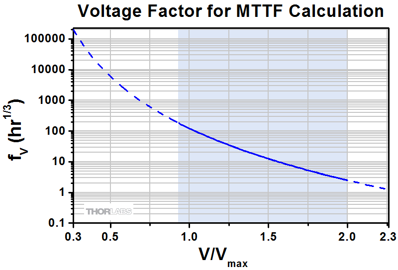
Quick changes in the applied voltage result in fast dimensional changes to the piezoelectric stack. The magnitude of the applied voltage determines the nominal extension of the stack. Assuming the driving voltage signal resembles a step function, the minimum time, Tmin, required for the length of the actuator to transition between its initial and final values is approximately 1/3 the period of resonant frequency. If there is no load applied to the piezoelectric stack, its resonant frequency is ƒo and its minimum response time is:

After reaching this nominal extension, there will follow a damped oscillation in the length of the actuator around this position. Controls can be implemented to mitigate this oscillation, but doing so may slow the response of the actuator.
Applying a load to the actuator will reduce the resonant frequency of the piezoelectric stack. Given the unloaded resonant frequency of the actuator, the mass of the stack, m, and the mass of the load, M, the loaded resonant frequency (ƒo') may be estimated:
Estimating Device Lifetime for DC Drive Voltage Conditions
The lifetime of a piezoelectric device is a function of the operating temperature, applied voltage, and relative humidity conditions. Lifetimes are reduced as a consequence of humidity-driven electrolytic reactions, which occur at the electrodes of the piezoelectric devices when a DC voltage is applied. These reactions both generate hydrogen and result in metal dendrites growing from the cathode towards the anode. The hydrogen liberated by the electrolytic reaction chemically reacts with and degrades the piezoelectric material. Dendrites that grow to electrically connect the cathode and anode result in increasing levels of leakage current. Failed piezoelectric devices are defined as those that exhibit leakage current levels above an established threshold.
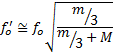
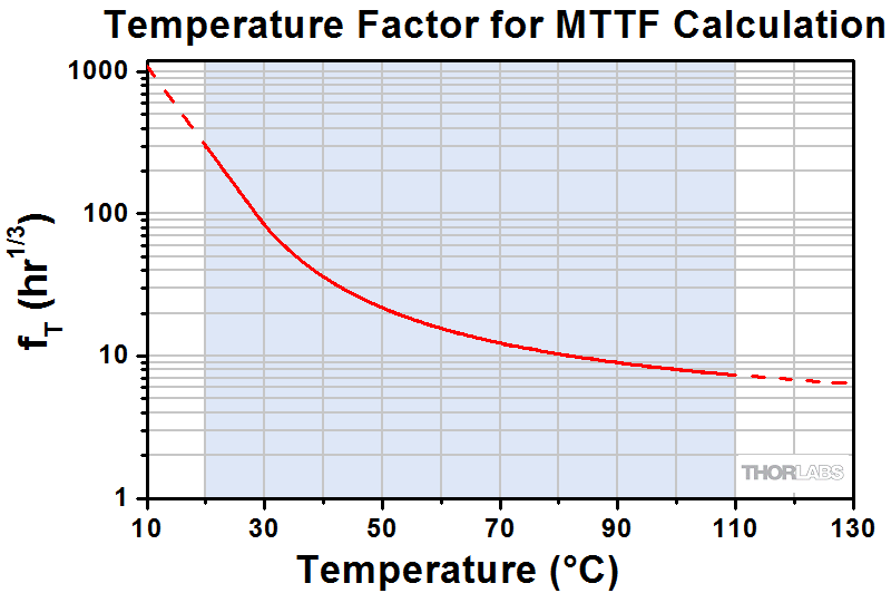
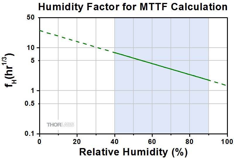
A ceramic moisture-barrier layer that insulates Thorlabs' piezoelectric devices on four sides is effective in minimizing the effects of humidity on device lifetime. As there is interest in estimating the lifetime of piezoelectric devices, Thorlabs conducted environmental testing on our ceramic-insulated, low-voltage, piezoelectric actuators. The resulting data were used to create a simple model that estimates the mean time to failure (MTTF), in hours, when the operating conditions of humidity, temperature, and applied voltage are known. The estimated MTTF is calculated by multiplying together three factors that correspond, respectively, to the operational temperature, relative humidity, and fractional voltage of the device. The fractional voltage is calculated by dividing the operational voltage by the maximum specified drive voltage for the device. The factors for each parameter can be read from the following plots, or they may be calculated by downloading the plotted data values and interpolating as appropriate.
In the following trio of plots, the solid-line segment of each curve represents the range of conditions over which Thorlabs performed testing. These are the conditions observed to be of most relevance to our customers. The dotted-line extensions to the solid-line segments represent extrapolated data and represent a wider range of conditions that may be encountered while operating the devices.
Click to Enlarge
Figure 2.2 For an Excel file containing these fT vs. temperature data, please click here.
Click to Enlarge
Figure 2.4 For an Excel file containing these fH vs. relative humidity data, please click here.
Click to Enlarge
Figure 2.3 For an Excel file containing these fV vs. V/Vmax data, please click here.
The data used to generate these temperature, voltage, and humidity factor plots resulted from the analysis of measurements obtained from testing devices under six different operational conditions. Different dedicated sets of ten devices were tested under each condition, with each condition representing a different combination of operational voltage, device temperature, and relative humidity. After devices exhibit leakage current levels above a threshold of 100 nA, they are registered as having failed. The individual contributions of temperature, humidity, and voltage to the lifetime are determined by assuming:
- MTTF = fV(V) * fT(T) * fH(H)
- A power law dependence for the voltage: fV(V) = A1Vb1
- An exponential relationship for the relative humidity: fH(T) = A2ecH
- An Arrhenius relationship for the temperature: fT(H) = A3eb2/T
where A1, A2, A3, b1, b2, and c are constants determined through analysis of the measurement data, V is the DC operational voltage, T is the device temperature, and H is the relative humidity. Because the MTTF has a different mathematical relationship with each factor, the dependence of the MTTF on each factor alone may be determined. This is the data plotted in Figures 2.2, 2.3, and 2.4. The regions of the curves marked by the blue shading are derived from experimental data. The dotted regions of the curves are extrapolated.
Lifetime testing of these devices continues, and additional data will be published here as they become available. To assist in temperature control, please see our selection of thermoelectric coolers. Temperature and humidity can be monitored using our USB Temperature and Humidity Logger.
| Posted Comments: | |
| No Comments Posted |
| Item #a,b | Info | Pre-Attached Wires |
Displacement (Free Stroke)c |
Stack Dimensionsd | Through Hole Diameter |
Resonant Frequencye |
Capacitance | Blocking Forcef | End Faces |
|---|---|---|---|---|---|---|---|---|---|
| PK4FA2H3P2 | Yes | 7.0 µm ± 15% | 5.0 mm x 5.0 mm x 9.0 mm | 2.0 mm | 140 kHz | 560 nF | 800 N (180 lbs) | Flat Plates | |
| PK4FTH3P2 | Yes | 20.0 µm ± 15% | 5.0 mm x 5.0 mm x 25.0 mm | 2.0 mm | 52 kHz | 1.3 µF | 800 N (180 lbs) | Flat Plates | |
| PK4FXH3P2 | Yes | 40.0 µm ± 15% | 5.0 mm x 5.0 mm x 50.0 mm | 2.0 mm | 26 kHz | 2.7 µF | 800 N (180 lbs) | Flat Plates | |
| PK4GA3H5P2 | Yes | 40.0 µm ± 15% | 7.0 mm x 7.0 mm x 45.0 mm | 3.0 mm | 30 kHz | 5.5 µF | 1600 N (360 lbs) | Flat Plates |
- All specifications are quoted at 25 °C, unless otherwise stated. For complete specifications, please see the Info Icons (
 ) above.
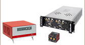
 - We recommend using the MDT69xB or KPC101 Open-Loop Controllers with these piezos. Our MPZ601 (≤75 V) or BPC30x Closed-Loop Controllers are also compatible. However, the actuators sold on this page do not contain a strain gauge and therefore will not provide positional feedback. If closed-loop feedback is needed, please consider our PK4FYC2 or PZS001 actuators.
- The "free stroke" displacement corresponds to no load.
- Stack dimensions exclude the electrodes, polyimide tape, and wire connection area.
- Without Load
- Specified at 150 V