 Products Home / Actuators, Adjusters, & Transducers / Piezoelectric Chips and Stacks / Round Piezoelectric Stacks and Chips, 2.8 µm to 12.0 µm Travel
Round Piezoelectric Stacks and Chips, 2.8 µm to 12.0 µm Travel

- Round Stacks and Chips with Ø5.0 mm or Ø8.3 mm
- Up to 12.0 µm Maximum Free Stroke Displacement
- Higher Drive Voltage and Displacement than Similar Square Piezos
- Longer Lifetime than Square Piezos for Identical Operating Conditions
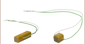
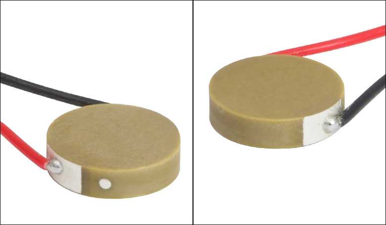
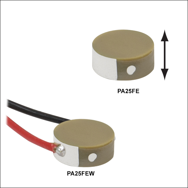
Silver Dot Indicates Positive Electrode
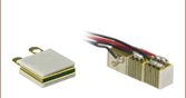
PK25FA2P2
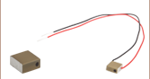
Ø5.0 mm Stack with Flat Ceramic End Plates,
75 mm Wires
PA25FEW
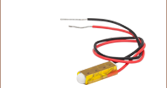
Ø5.0 mm Chip, 75 mm Wires
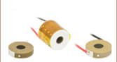
PA25LE
Ø8.3 mm Chip, Bare Electrodes
Arrows Indicate Direction of Expansion
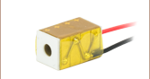
PA25FE
Ø5.0 mm Chip, Bare Electrodes
PKLEQ5
Ø8.3 mm, 0.5 mm Thick End Plate


Please Wait
| Piezo Selection Guide |
|---|
| Piezoelectric Ceramic Chips |
| Square |
| Square with Through Hole |
| Round |
| Ring |
| Tube |
| Shear |
| Benders |
| Single-Crystal Piezoelectric Chips |
| Square |
| Piezoelectric Ceramic Stacks |
| Discrete, Square |
| Discrete, Square with Through Hole |
| Discrete, Round |
| Discrete, Ring |
| Discrete, Hermetically Sealed |
| Discrete, Shear (1D to 3D Positioners) |
| Co-Fired: Square, Square with Through Hole, Round, & Ring |
| Co-Fired or Discrete: Square with Strain Gauges |
| Piezoelectric Crystal Stacks |
| Square |
| Mounted Piezoelectric Actuators |
| Ultrasonic Piezo Chips & Transducers |
| Vibrating Piezo Actuator |
Click to Enlarge
Figure 1.1 A silver dot indicates the positive electrode (left). There is no mark next to the negative electrode (right).
Features
- Round Piezo with Ø5.0 mm or Ø8.3 mm Cross Section
- Chips with Bare Electrodes or Pre-Attached Wires
- Discrete Stacks with Flat Ceramic End Plates and Pre-Attached Wires
- Drive Voltage Range of 0 - 200 V
- For Use in Open-Loop Setups
- Ideal for Vacuum and OEM Applications
- Custom Options Available; Please Contact Tech Support
- Flat End Plates Available Separately
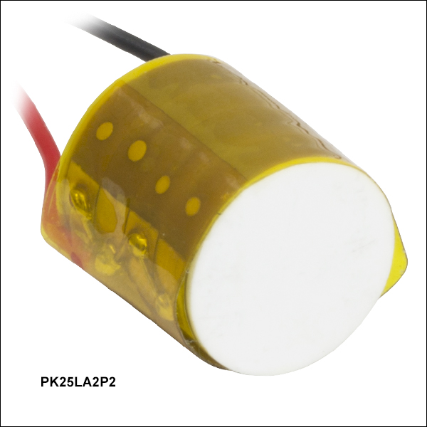
Thorlabs' round piezoelectric actuators are offered as a chip with bare electrodes, a chip with pre-attached wires, or as a discrete stack consisting of multiple chips bonded via epoxy and glass beads. The wired and unwired chips are available with a Ø5.0 mm or Ø8.3 mm, providing a maximum free stroke of 2.8 µm or 3.3 µm, respectively, when driven to 200 V. The Ø5.0 mm discrete stacks provide 11.0 µm of travel when driven to 200 V, while the Ø8.3 mm stacks provide 12.0 µm of travel when driven to 200 V. For convenience, 75 mm wires are attached to the PA25FEW chip, PA25LEW chip, PK25FA2P2 stack, and PK25LA2P2 stack. The flat endfaces of the discrete stacks are fitted with ceramic end plates. With their compact dimensions and light weight, these piezos can easily be integrated into systems for precision movement. Through a precision grinding process, the accuracy of the design height is ensured to better than ±5 µm.
Round vs. Square Piezos
Round piezoelectric actuators have several advantages when compared with their square counterparts. The round geometry allows the load to be uniformly distributed across the surface, while square piezo actuators experience stress concentration at their sharp corners. This concentration of stress can make the actuator crack more easily, which can cause the piezo to fail. Greater immunity from stress-induced cracking allows round chips to be fabricated with thinner active layers than the square piezoelectric actuators. Our design is optimized to provide round piezo actuators with the longest stroke. In addition, round piezo actuators have longer lifetimes than square piezo actuators when they are operated under the same conditions, and the round actuators can be driven by higher voltages. These round piezos have a maximum rated drive voltage of 200 V, while their square counterparts have drive voltages rated up to 150 V. Piezo actuators with square cross sections may be preferred over round piezos when an actuator with a rectangular shape is more easily accommodated, such as in a square corner, or when lower-cost actuators are desired.
Piezo Chip Construction and Operation
Piezo chips are fabricated from a series of stacked piezoelectric ceramic layers. An electrode is screen-printed on each layer, and the printed layers are isostatically pressed together to create a chip. The electrodes are electrically in parallel. Each chip has an insulating ceramic layer sealing the outer and inner diameters, as well as the flat top and bottom surfaces. The drive voltage is applied to two screen printed electrodes located on the outer diameter of the ring. For these chips and stacks, a silver dot indicates the positive electrode that should receive positive bias, as is shown in the image at the top of this section. In the case of the wired actuators, the wire soldered to this electrode is red.

The maximum displacement of these actuators is achieved when they are preloaded with the maximum displacement load, which is specified for each product. The actual value of the maximum displacement varies for each item and must be experimentally determined; however, the maximum displacement will always be larger than the free stroke displacement. Please note that when mounting a load onto the piezoelectric chip, the force should be directed along the actuator's axis of displacement. For more details, see the Operation tab.
Thorlabs' piezoelectric chips are individually inspected using a proprietary AI algorithm to ensure the highest quality of our line of piezo chips, actuators, and transducers.
To accommodate a variety of loading conditions, flat ceramic end plates may be purchased as accessories for the piezoelectric chips below.
Piezo chips with custom dimensions, voltage ranges, and coatings are available. Additionally, customers can order these piezo chips in high-volume quantities. Please contact Tech Support for more information.

Click to Enlarge
Dicing the PZT Block into Individual Elements
Click to Enlarge
Chips After Binder Burnout and Sintering
Thorlabs' In-House Piezoelectric Manufacturing
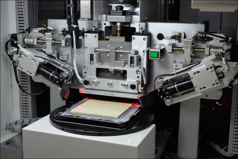
Our piezoelectric chips are fabricated in our production facility in China, giving us full control over each step of the manufacturing process. This allows us to economically produce high-quality products, including custom and OEM devices. A glimpse into the fabrication of our piezoelectric chips follows. For more information about our manufacturing process and capabilities, please see our Piezoelectric Capabilities page.
- Build Blocks from Flexible Sheets of Lead Zirconate Titanate (PZT) or BiScO3-PbTiO3 (BSPT) Powder
- Screen Print Electrodes on Each Individual Sheet
- Layer the Printed Sheets One Top of Another
- Consolidate the Layered Sheets in an Isostatic Press
- Dice the Block into Individual Elements
- Purge Solvent and Binder Material Residues by Heat Treating the Elements
- Sinter the Elements to Fuse the Piezoelectric Pressed Powder and Grow PZT or BSPT Crystals
- Lap the Elements to Achieve Tight Dimensional Tolerances: ±5 µm for Each Element
- Screen Print the Outer Electrodes on the Elements
- Align the Individual PZT or BSPT Crystals Along the Same Axis by Poling the Elements
Operation Notes
Click to Enlarge
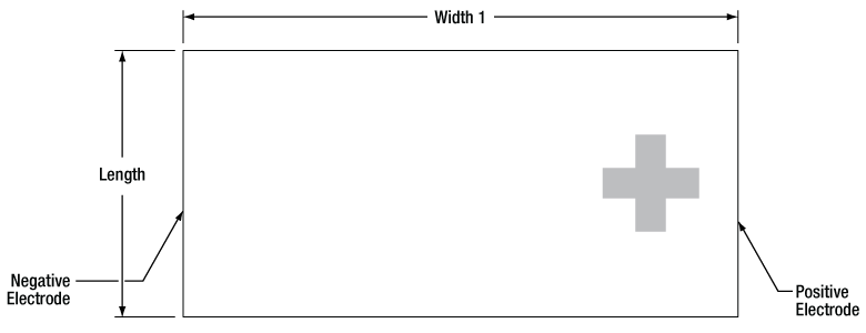
Figure 2.1 Schematic of TA0505D024W Piezo Chip Showing the + Mark Close to the Positive Electrode
Click to Enlarge
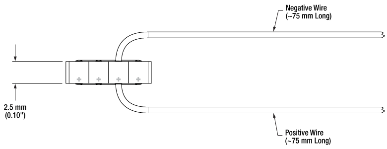
Figure 2.2 Schematic of PK4DMP2 Piezo Stack Showing the Line of + Marks Close to the Positive Electrode
Power Connections
A positive bias should be applied across the device. The positive electrode should receive positive bias, and the other electrode should be connected to ground. Applying a negative bias across the device may cause mechanical failure. For products that ship with wires attached, the positive wire is red, as can be seen in the product images. For pre-wired chips, the red wire is attached to the electrode that is identified by a + mark, as is depicted in Figure 2.1. (On some devices, a silver dot indicates the positive electrode.) On stacks, the red wire is attached to electrode on the side of the stack indicated by the line of + marks (or silver dots), as is depicted in Figure 2.2. The wire that should be grounded is black, and it is attached to the electrode on the side of the chip opposite the side with the positive electrode.
Caution: After driving, the piezo is fully charged. Directly connecting the positive and negative electrodes has the risk of electricity discharging, spark, and even failure. We recommend using a resistor (>1 kΩ) between the wires to release the charge.
Preloading
The maximum displacement of these actuators is achieved when they are preloaded with the maximum displacement load, which is specified for each product. The actual value of the maximum displacement varies for each item and must be experimentally determined; however, the maximum displacement will always be larger than the free stroke displacement. Preloading increases the length of the actuator's stroke because the poling process performed during fabrication does not align all ferroelectric grains in the piezoelectric material in the same direction. Preloading the actuator mechanically forces many of the mis-aligned grains into a more ideal alignment. Applying a driving voltage across the piezo material causes the orientations of the ferroelectric grains to rotate so they become aligned with the applied field, and this results in a dimensional change of the piezo material. When more ferroelectric grains are initially aligned in the same direction, the dimensional change of the piezo material in response to the applied driving voltage is greater. Preloads greater than the optimal maximum displacement load result in displacements less than the maximum displacement, as higher loads oppose the switching of the grain orientations in response to the applied driving voltage.
Soldering Wire Leads to the Electrodes
If wire leads must be reattached to the electrodes, a soldering temperature no higher than 370 °C (700 °F) should be used, and heat should be applied to each electrode for a maximum of 2 seconds. Solder the lead to the middle of the electrode and keep the region over which heat is applied as small as possible.
Interfacing a Piezoelectric Element with a Load
Piezoceramics are brittle and have low tensile strength. Avoid loading conditions that subject the actuator to lateral, transverse, or bending forces. When applied incorrectly, an external load that may appear to be compressive can, through bending moments, cause high tensile stresses within the piezoelectric device. Improperly mounting a load to the piezoelectric actuator can easily result in internal stresses that will damage the actuator. To avoid this, the piezoelectric actuator should be interfaced with an external load such that the induced force is directed along the actuator's axis of displacement. The load should be centered on and applied uniformly over as much of the actuator's mounting surface as possible. When interfacing the flat surface of a load with an actuator capped with a flat mounting surface, ensure the two surfaces are highly flat and smooth and that there is good parallelism between the two when they are mated. If the external load is directed at an angle to the actuator's axis of displacement, use an actuator fitted with a hemispherical end plate or a flexure joint to achieve safe loading of the piezoelectric stack.

Click to Enlarge
Figure 2.4 Loads properly and improperly mounted to piezo actuators using a variety of interfacing methods.
To accommodate a variety of loading conditions, flat ceramic end plates may be purchased as accessories for these chips. To attach a load to PZT piezo chips, we recommend using an epoxy that cures at a temperature lower than 80 °C (176 °F), such as our 353NDPK or TS10 epoxies or Loctite® Hysol® 9340. For BiScO3-PbTiO3 (BSPT) piezo chips, we recommend any inorganic adhesive which cures at a temperature lower than 120 °C and has a melting point higher than 250 °C; our 353NDPK epoxy is safe to use, however the strength will be reduced at 250 °C, and therefore a preload should be applied to maintain the mechanical structure. Loads should be mounted only to the faces of the piezoelectric chip that translate. Mounting a load to a non-translating face may lead to the mechanical failure of the actuator. Some correct and incorrect approaches to interfacing loads with piezoelectric actuators are discussed in the following paragraphs.
Click to Enlarge
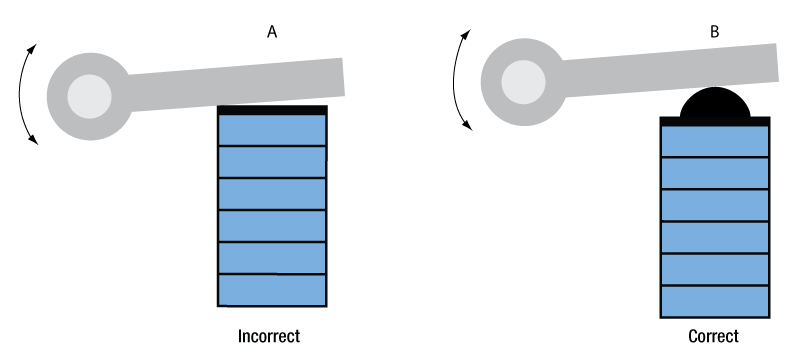
Figure 2.3 Actuation of a lever arm using stack fitted with a flat plate
(A, Incorrect), and a hemispherical plate (B, Correct).
Figure 2.3 presents incorrect (A) and correct (B) methods for using a piezoelectric stack to actuate a lever arm. The correct method uses a hemispherical end plate so that, regardless of the angle of the lever arm, the force exerted is always directed along the translational axis of the actuator. The incorrect interfacing of the stack and the lever arm, shown in Figure 2.3 (A), endangers the stack by applying the full force of the load to one edge of the stack. This uneven loading causes dangerous stresses in the actuator, including a bending moment around the base.
Figure 2.4 shows an example of an incorrect (A) and correct (B) approach for interfacing a flat-bottomed, off-axis load with a piezoelectric actuator. Approach A is similar to the incorrect approach shown in Figure 2.3. In correct approach B, a flexure mount acts as an interface between the off-axis flat mounting surface of the load and the flat mounting plate of the actuator. The flexure mount ensures that the load is both uniformly distributed over the surface plate of the actuator and that the loading force is directed along the translational axis of the actuator.
Operating Under High-Frequency Dynamic Conditions
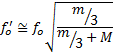
It may be necessary to implement an external temperature-control system to cool the device when it is operated at high frequencies. The maximum operating temperature of PZT piezos is 130 °C (266 °F), and high-frequency operation causes the internal temperature of the piezoelectric device to rise. For higher temperature applications, BSPT piezos are available with a maximum operating temperature of 250 °C. The dependence of the device temperature on the drive voltage frequency for each product can be accessed by clicking the Info icons, ![]() in Tables G1.1 and G2.1. The temperature of the device should not be allowed to exceed its specified maximum operating temperature.
in Tables G1.1 and G2.1. The temperature of the device should not be allowed to exceed its specified maximum operating temperature.
Estimating the Resonant Frequency for a Given Applied Load
A parameter of significance to many applications is the rate at which the piezoelectric actuator changes its length. This dimensional rate of change depends on a number of factors, including the actuator's resonant frequency, the absolute maximum bandwidth of the driver, the maximum current the piezoelectric device can produce, the capacitance of the piezoelectric stack, and the amplitude of the driving signal. The length of the voltage-induced extension is a function of the amplitude of the applied voltage driving the actuator and the length of the piezoelectric stack. The higher the capacitance, the slower the dimensional change of the actuator.
Quick changes in the applied voltage result in fast dimensional changes to the piezoelectric stack. The magnitude of the applied voltage determines the nominal extension of the stack. Assuming the driving voltage signal resembles a step function, the minimum time, Tmin, required for the length of the actuator to transition between its initial and final values is approximately 1/3 the period of resonant frequency. If there is no load applied to the piezoelectric stack, its resonant frequency is ƒo and its minimum response time is:

After reaching this nominal extension, there will follow a damped oscillation in the length of the actuator around this position. Controls can be implemented to mitigate this oscillation, but doing so may slow the response of the actuator.
Applying a load to the actuator will reduce the resonant frequency of the piezoelectric stack. Given the unloaded resonant frequency of the actuator, the mass of the stack, m, and the mass of the load, M, the loaded resonant frequency (ƒo') may be estimated:

Click to Enlarge
Figure 2.5 Diagram of Piezo Stack Insulation Methods:
(a) In-Chip Insulation Used in Standard Chips and Discrete Stacks,
(b) On-Stack Insulation Used in Co-Fired Stacks
Co-Fired Piezo Chips, Co-Fired Piezo Stacks, and Discrete Piezo Stacks
Generally speaking, Thorlabs' co-fired piezo chips and stacks are constructed similarly. In both cases, a structure is built up from alternating electrode layers and green-state lead zirconate titanate (PZT) piezoelectric layers. (The co-fired piezo chips are also available with BiScO3-PbTiO3 (BSPT) piezoelectric layers for higher temperature applications.) The assembled structure is then sintered into a single monolithic unit. Supply electrodes of opposite polarity are attached to opposite sides of the structure. Each internal electrode is electrically coupled to one or the other supply electrode, such that no two adjacent internal electrodes have the same polarity. The most significant differences between the co-fired chips and stacks arise from the way each internal electrode is electrically isolated from the supply electrodes of opposite polarity. The different electrical insulation approaches influence the mechanical properties of the actuators. Actuators fabricated using the two different approaches are diagrammed in Figure 2.5.
In the case of the chips (In-Chip Insulation), the internal electrodes of opposite polarities alternate. Each internal electrode layer is shorter than the full width of the piezo layer. All electrodes of one polarity have edges that are flush with one side of the chip, and all electrodes with the opposite polarity are flush with the opposite side of the chip. Because the electrode does not extend all the way to the opposite edge, the far end of the electrode is completely surrounded by PZT or BSPT material. The PZT or BSPT material enclosing the end of the electrode is insulating, which electrically isolates this electrode from the supply electrode of opposite polarity. This approach to electrically insulating the electrodes creates a region of stress at the edge of the electrode. The stress arises both due the abrupt change in thickness on either side of the electrode edge, as well as the tensile stress created when the PZT or BSPT material sandwiched between electrodes responds to an applied voltage drive signal, but the insulating PZT or BSPT material beyond the edge of the electrodes does not. This stress limits the maximum height of chips manufactured using this approach. The height of chips are limited to ensure internal stresses are low and do not affect lifetime or performance. Chips are sealed in a ceramic layer that offers superior resistance to humidity and heat than epoxy resin coatings.
One way of increasing the height, and therefore the maximum stroke, of piezo actuators based on these chips is to fabricate discrete piezo stacks. These are manufactured by bonding multiple chips together in series using a glass-bead epoxy. Discrete stacks can be fabricated to substantially longer lengths than co-fired chips or stacks, and this allows them to achieve higher maximum displacements while maintaining sub-millisecond response times and a low drive voltage range. As the constituent chips are sealed within a ceramic barrier layer, discrete stacks have superior resistance to humidity and heat than co-fired stacks, which are sealed in an epoxy resin coating.
In the case of co-fired stacks (On-Stack Insulation), the electrodes extend across the full width of the PZT layers. The edges of the electrodes are flush with all four sides of the stack, including the side with the supply electrode of opposite polarity. The edge of the internal electrode is insulated from that supply electrode by a layer of glass filament applied to the side of the stack. Precision localized application of the glass filament ensures that the electrode edge is electrically isolated from the supply electrode, and that the filament is applied over minimal surface area; the ability of the supply electrode to make electrical connections to the desired internal electrodes is not affected, and the small amount of applied glass filament does not affect the operation of the actuator. With their full-width electrodes, piezo actuators made using this insulating approach are characterized by homogeneous internal stress. Co-fired stacks can therefore be fabricated with greater heights than chips fabricated using the in-chip insulation approach. Co-fired stacks also have a higher percentage of active PZT material than the discrete stacks, which include inactive bonding layers of glass-bead epoxy. They are coated in an epoxy resin.
Estimating Device Lifetime for DC Drive Voltage Conditions
The lifetime of a piezoelectric device is a function of the operating temperature, applied voltage, and relative humidity conditions. Lifetimes are reduced as a consequence of humidity-driven electrolytic reactions, which occur at the electrodes of the piezoelectric devices when a DC voltage is applied. These reactions both generate hydrogen and result in metal dendrites growing from the cathode towards the anode. The hydrogen liberated by the electrolytic reaction chemically reacts with and degrades the piezoelectric material. Dendrites that grow to electrically connect the cathode and anode result in increasing levels of leakage current. Failed piezoelectric devices are defined as those that exhibit leakage current levels above an established threshold.
A ceramic moisture-barrier layer that insulates Thorlabs' piezoelectric devices on four sides is effective in minimizing the effects of humidity on device lifetime. As there is interest in estimating the lifetime of piezoelectric devices, Thorlabs conducted environmental testing on our ceramic-insulated, low-voltage, piezoelectric actuators. The resulting data were used to create a simple model that estimates the mean time to failure (MTTF), in hours, when the operating conditions of humidity, temperature, and applied voltage are known. The estimated MTTF is calculated by multiplying together three factors that correspond, respectively, to the operational temperature, relative humidity, and fractional voltage of the device. The fractional voltage is calculated by dividing the operational voltage by the maximum specified drive voltage for the device. The factors for each parameter can be read from the following plots, or they may be calculated by downloading the plotted data values and interpolating as appropriate.
In the following trio of plots, the solid-line segment of each curve represents the range of conditions over which Thorlabs performed testing. These are the conditions observed to be of most relevance to our customers. The dotted-line extensions to the solid-line segments represent extrapolated data and represent a wider range of conditions that may be encountered while operating the devices.
Click to Enlarge
Figure 2.6 For an Excel file containing these fT vs. temperature data, please click here.
Calculation of MTTF to Estimate Lifetimes: MTTF = fV * fT * fH
As an example, when a device of type PK2FSF1 is operated with a voltage of 60 V, at a temperature of 30 °C, and in an environment with 75% relative humidity:
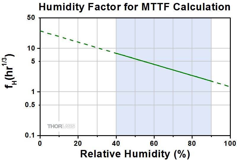
- From Figure 2.7, the voltage factor is 427 (The maximum rated voltage, Vmax, of the PK2FSF1 is 75 V, giving V/Vmax = 60 V / 75 V = 0.80.)
- From Figure 2.6, the temperature factor is 83
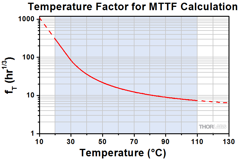
- From Figure 2.8, the humidity factor is 2.8
Then MTTF = 472 * 83 * 2.8 = 99234.8 hours, which is greater than 11 years.
Note that relationships graphed on this page apply only to Thorlabs' ceramic-insulated, low-voltage, piezoelectric stack actuators.
Click to Enlarge
Figure 2.8 For an Excel file containing these fH vs. relative humidity data, please click here.
Click to Enlarge
Figure 2.7 For an Excel file containing these fV vs. V/Vmax data, please click here.
The data used to generate these temperature, voltage, and humidity factor plots resulted from the analysis of measurements obtained from testing devices under six different operational conditions. Different dedicated sets of ten devices were tested under each condition, with each condition representing a different combination of operational voltage, device temperature, and relative humidity. After devices exhibit leakage current levels above a threshold of 100 nA, they are registered as having failed. The individual contributions of temperature, humidity, and voltage to the lifetime are determined by assuming:
- MTTF = fV(V) * fT(T) * fH(H)
- A power law dependence for the voltage: fV(V) = A1Vb1
- An exponential relationship for the relative humidity: fH(T) = A2ecH
- An Arrhenius relationship for the temperature: fT(H) = A3eb2/T
where A1, A2, A3, b1, b2, and c are constants determined through analysis of the measurement data, V is the DC operational voltage, T is the device temperature, and H is the relative humidity. Because the MTTF has a different mathematical relationship with each factor, the dependence of the MTTF on each factor alone may be determined. These are the data plotted in Figures 2.6 through 2.8. The regions of the curves in Figures 2.6 through 2.8 marked by the blue shading are derived from experimental data. The dotted regions of the curves are extrapolated.
Lifetime testing of these devices continues, and additional data will be published here as they become available. To assist in temperature control, please see our selection of thermoelectric coolers. Temperature and humidity can be monitored using our USB Temperature and Humidity Logger.
Cleaning for Vacuum Compatibility
When suitable for vacuum applications, Thorlabs' piezo chips have the rated vacuum compatibility specified in their Info Icons (![]() ). While no extra cleaning is needed to achieve this value, we recommend cleaning these products with isopropyl alcohol (IPA) in an ultrasonic immersion tank and then baking them at 60 °C for two hours. Do not immerse the device in other organic solvents.
). While no extra cleaning is needed to achieve this value, we recommend cleaning these products with isopropyl alcohol (IPA) in an ultrasonic immersion tank and then baking them at 60 °C for two hours. Do not immerse the device in other organic solvents.
| Posted Comments: | |
Joseph Purvis
(posted 2025-03-18 11:45:00.167) Can you please tell me what the material for this product is eg PZT4, PZT5H, BaTiO3, LiNbO3 or something else?
I've purchased three devices and there's no information on the datasheet.
Thank you cdolbashian
(posted 2025-03-20 02:24:59.0) Thank you for contacting us with this inquiry. The material of these piezo stacks is THP51, which is mostly close to the PZT5H. 捷 徐
(posted 2022-08-29 19:14:06.69) 这款产品的重复性如何? cdolbashian
(posted 2022-09-07 03:00:59.0) Thank you for contacting Thorlabs. Unlike conventional motor actuators, the stroke of the piezo actuator will demonstrate hysteresis in an open-loop system. The exact shape and characteristics of the hysteresis is heavily dependent upon the applied voltage difference as well as environmental and system conditions such as temperature or the applied load. Experiences suggest that, during a 1000 cycles’ testing under stable condition, the displacement’s variation is less than 5%. Closed-loop system can essentially eliminate the hysteresis using a feedback loop. The piezo hysteresis graphs can be found by clicking on the blue icon in spec table. lwest
(posted 2017-09-15 00:22:15.777) Is it possible to run this device at any negative voltage? I would like to apply -5V to 5V in my application. tfrisch
(posted 2017-09-26 02:53:54.0) Hello, thank you for contacting Thorlabs. Axial piezo chips and stacks should not be driven at negative voltages, so you should add a DC bias to your drive signal to make the minimum value zero. |

 Zoom
Zoom| Table G1.1 Specifications | |||||||||
|---|---|---|---|---|---|---|---|---|---|
| Item #a | Info | Pre-Attached Wires |
Displacement (Free Stroke)b |
Dimensionsc | Resonant Frequency |
Load for Maximum Displacementd |
Capacitance | Blocking Forcee |
End Faces |
| PA25FE | No | 2.8 µm ± 15% | Diameter: 5.0 mm ± 0.1 mm Length: 2.0 mm ± 5 µm |
350 kHz | 310 N (70 lbs) | 150 nF ± 15% | 780 N (175 lbs) |
No Plates | |
| PA25FEW | Yes | ||||||||
| PA25LE | No | 3.3 µm ± 15% | Diameter: 8.3 mm ± 0.1 mm Length: 2.0 mm ± 5 µm |
235 kHz | 720 N (162 lbs) | 580 nF ± 15% | 1800 N (405 lbs) |
No Plates | |
| PA25LEW | Yes | ||||||||
| Webpage Features | |
|---|---|
| Clicking this icon opens a window containing item-specific specifications and mechanical drawings. | |

 Zoom
Zoom| Table G2.1 Specifications | |||||||||
|---|---|---|---|---|---|---|---|---|---|
| Item #a | Info | Pre-Attached Wires |
Displacement (Free Stroke)b |
Dimensionsc | Resonant Frequency |
Load for Maximum Displacementd |
Capacitance | Blocking Forcee |
End Faces |
| PK25FA2P2 | Yes | 11.0 µm ± 15% | Diameter: 5.0 mm ± 0.1 mm Length: 9.0 mm ± 0.1 mm |
135 kHz | 310 N (70 lbs) | 570 nF ± 15% | 780 N (175 lbs) | Flat Plates | |
| PK25LA2P2 | Yes | 12.0 µm ± 15% | Diameter: 8.3 mm ± 0.1 mm Length: 9.0 mm ± 0.1 mm |
125 kHz | 720 N (162 lbs) | 2.2 µF ± 15% | 1800 N (405 lbs) | Flat Plates | |
| Webpage Features | |
|---|---|
| Clicking this icon opens a window containing item-specific specifications and mechanical drawings. | |

 Zoom
Zoom| Table G3.1 Circular End Plates | ||||
|---|---|---|---|---|
| Item # | Diameter | Thickness | Tolerance | Compatible Piezo Chips |
| PKFEQ5 | 5.00 mm | 0.50 mm | ±0.04 mm | PA25FE(W) |
| PKLEQ5 | 8.30 mm | 0.50 mm | ±0.04 mm | PA25LE(W) |
- Flat End Plates in Two Sizes
- Spread Force Across Piezo Face at Contact Point
- Sold in Packs of 16
The flat plates used in the piezo stacks featured above are also available separately in three sizes for compatibility with select piezo chips (see Table G3.1). Flat end plates are used to spread the force at the contact point over the entire end surface of a piezo stack or chip. When selecting a flat end plate to adhere to a piezo end face, it is important to match the bottom surface area of the plate to the cross section of the piezo in order to ensure that forces are spread evenly over the surface. These flat end plates have a dimensional tolerance of ±0.04 mm.